Magnetic Fuel Level Sensing
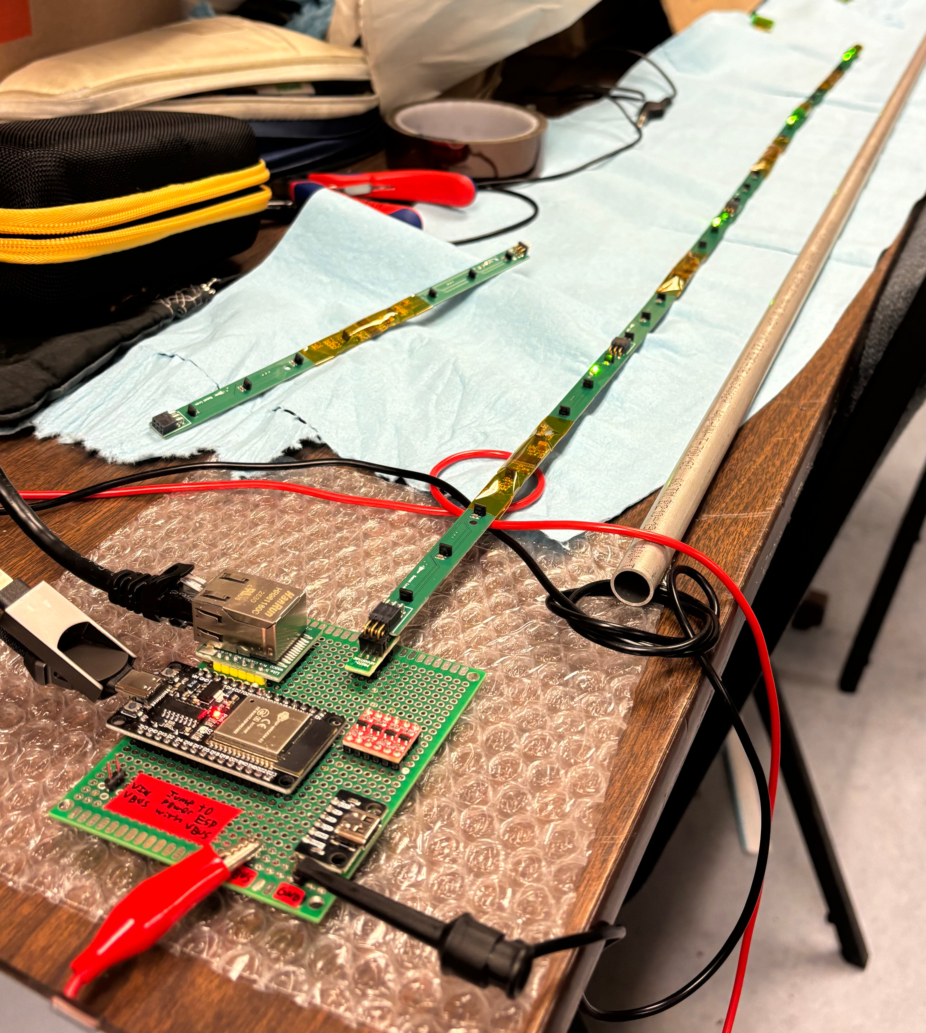
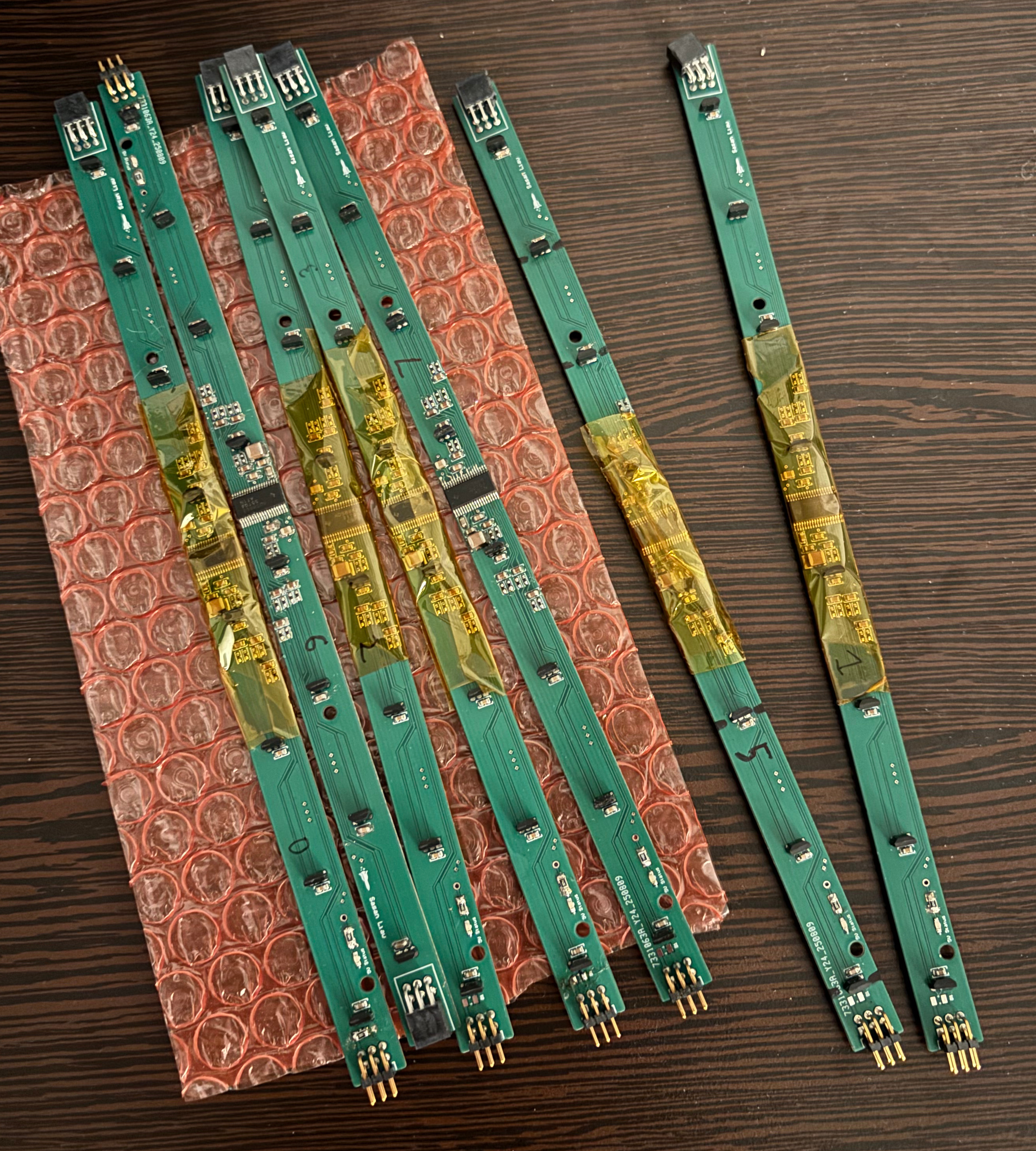
As a member of Space Enterprise at Berkeley, UC Berkeley’s liquid rocketry team, I designed a modular sensor array that contactlessly measures the amount of propellant in the engine test stand's fuel tank. The current version consists of several Hall effect sensor modules and a main controller board.
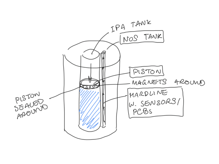
The system measures fuel level by tracking a magnetic piston inside the tank that falls as the propellant is consumed. The Hall effect sensors output a lower voltage when the magnet nears them, allowing the piston’s position to be precisely calculated. Prior to integration into the tank, it demonstrated ±0.25 cm positional accuracy and can reliably track a magnet moving linearly alongside the sensor array. The array’s length is adjustable and has been validated to function at up to 100 cm. After integration, it has also operated successfully during live engine tests.


.png)
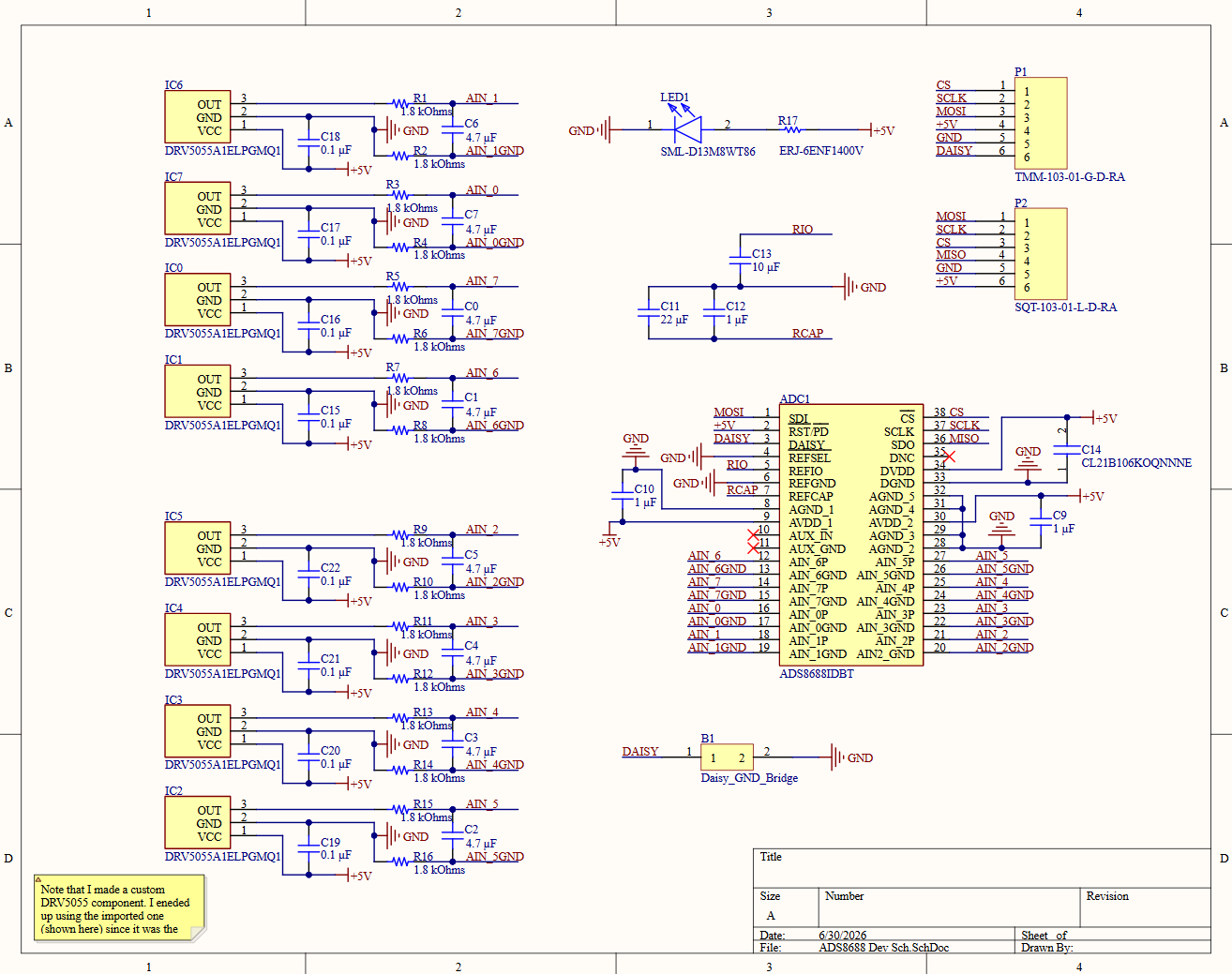
I designed each sensor module to be a self-contained PCB consisting of eight DRV5055 Hall effect sensors and one ADS8668 daisy-chainable ADC. The identical sensor modules can connect to one another, allowing the array to scale to the required length. The daisy-chainable ADCs allow data to be transferred serially up the chain and to the controller. They communicate using the SPI protocol.
Having an ADC on each individual module simplifies circuitry, as fewer lines need to cross the entire length of the chain. It also improves signal integrity by converting analog readings to digital values before passing them up the chain, minimizing data errors from voltage drops along the trace.
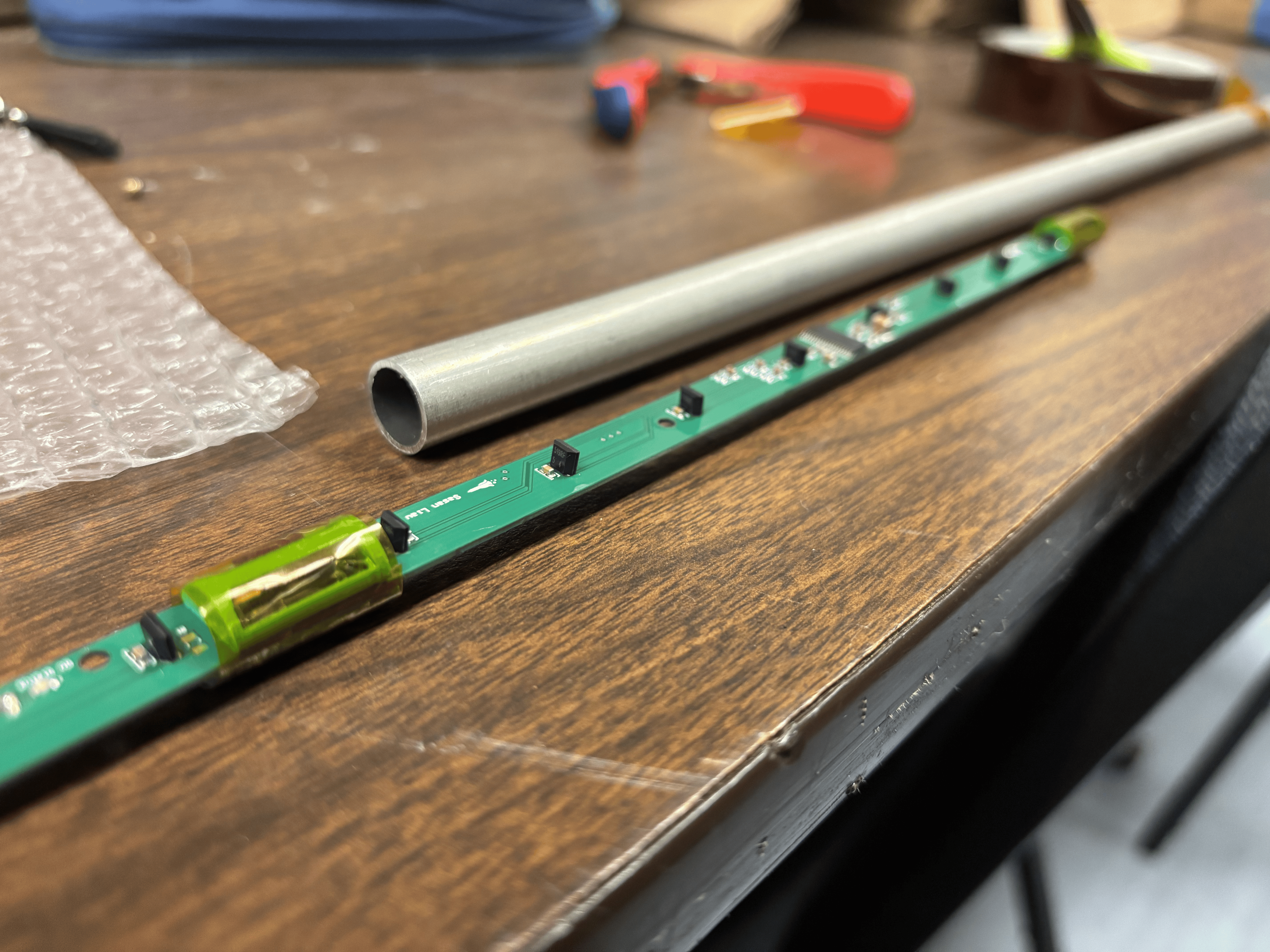
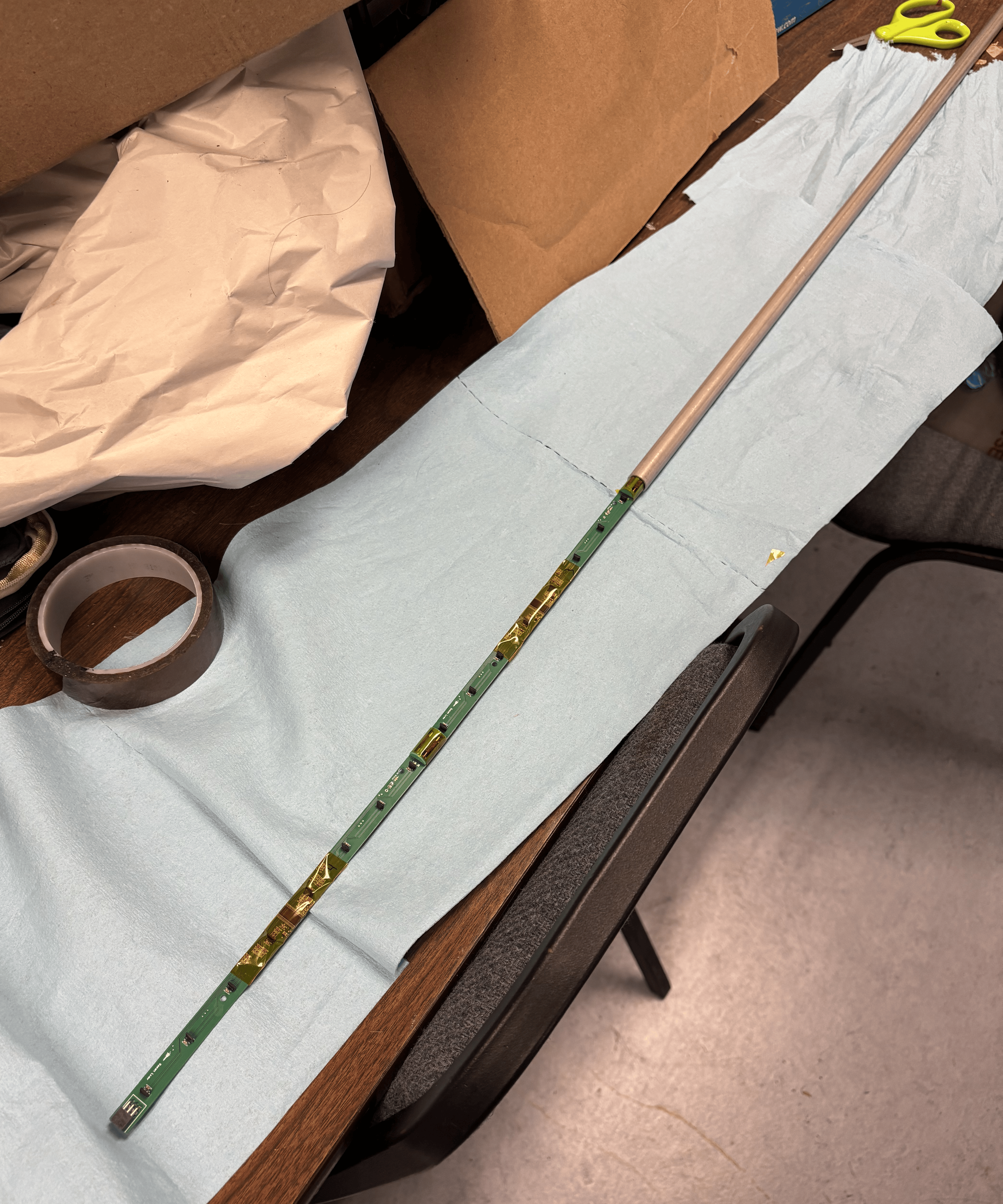
Additionally, I designed the sensor modules to fit within a strict 11mm width constraint, allowing them to slide into an aluminum tube mounted directly outside the tank. This was the only feasible mounting option due the tank’s existing design.
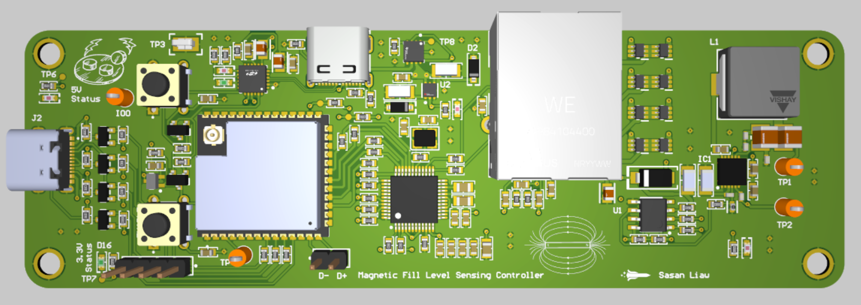
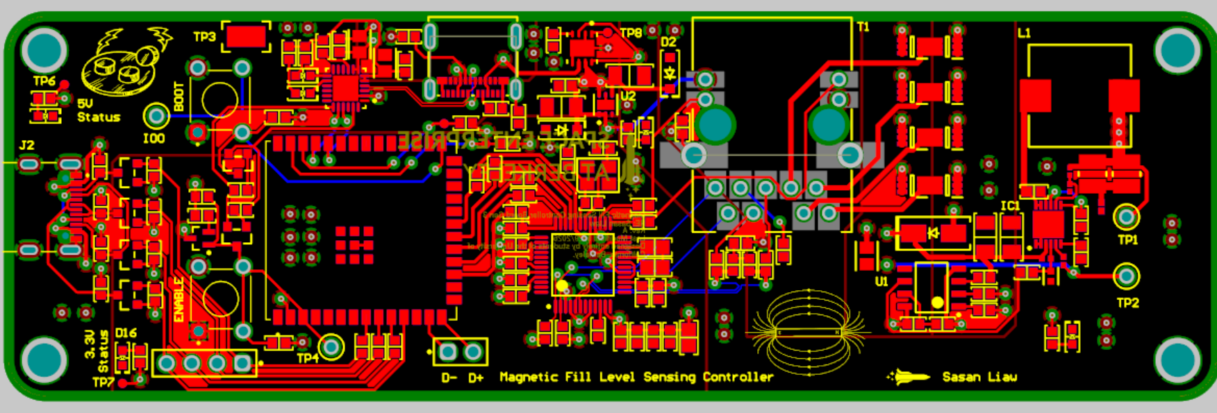
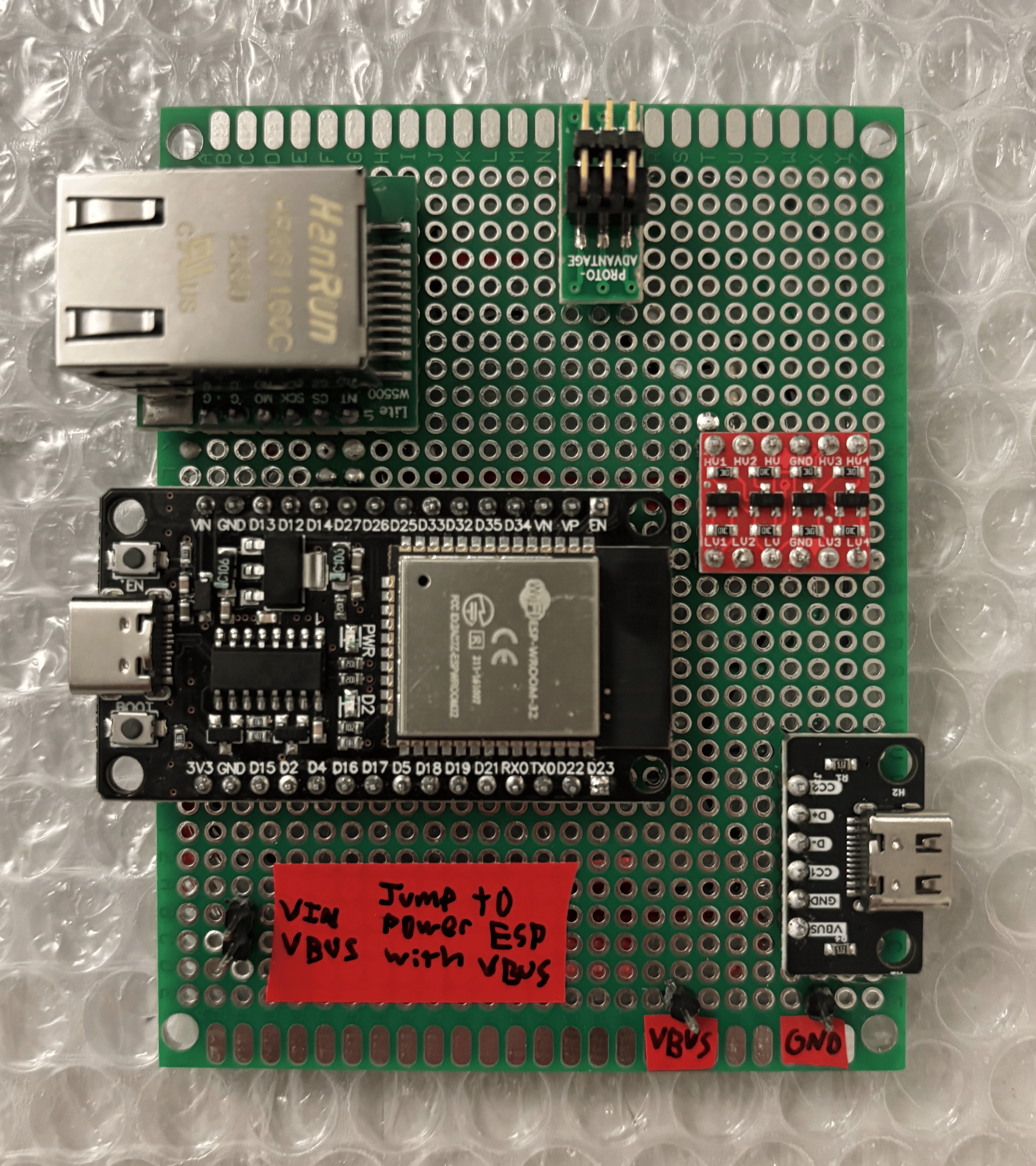
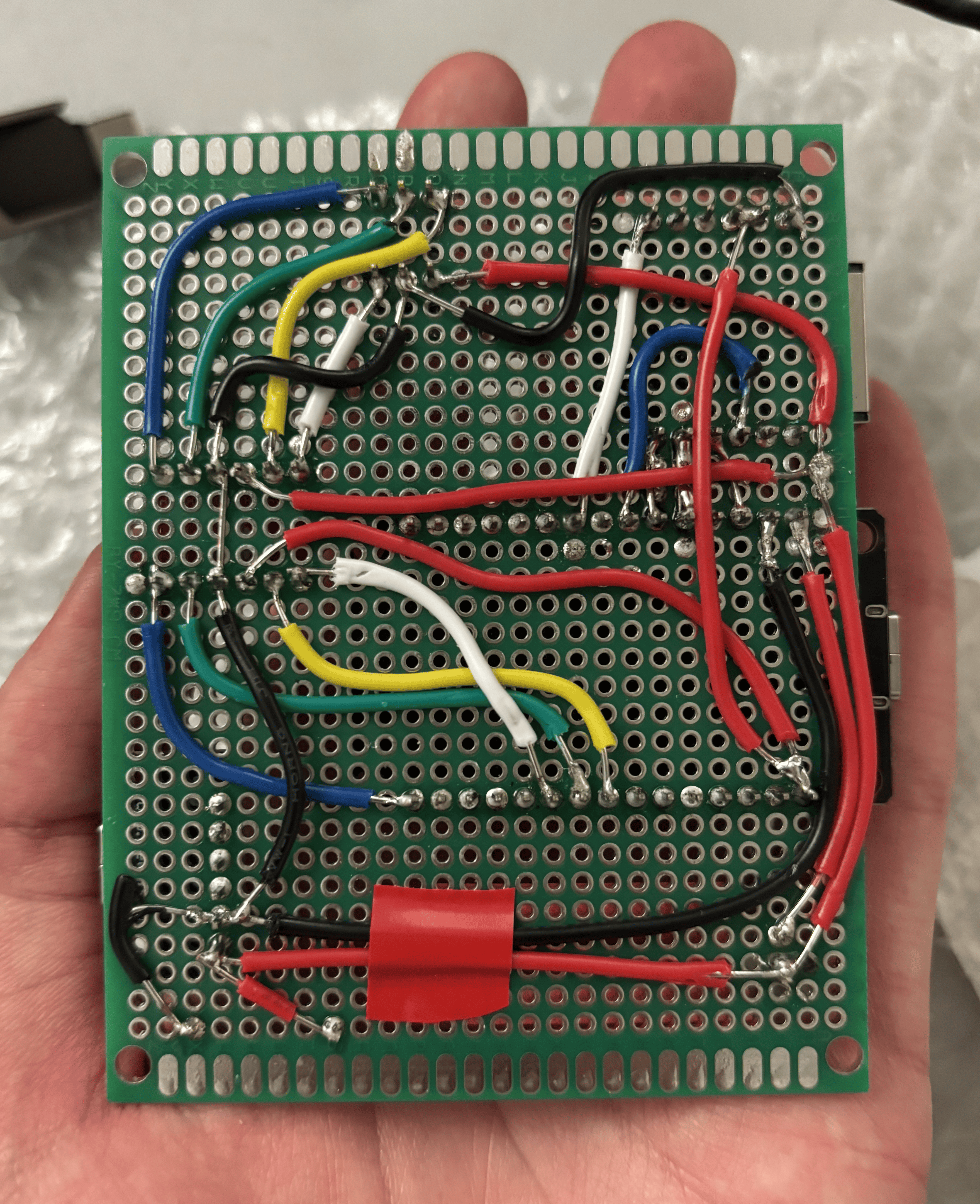
The controller is a separate board featuring an ESP32 microcontroller, Power over Ethernet (PoE) circuitry, and logic level shifters (the MCU works at 3.3V while the ADCs are at 5V). It distributes power from PoE to the sensor modules, sends configuration data, and manages data transfer. I initially designed a PCB to achieve this but it requires further iteration before deployment. A protoboard is currently being used to verify the system’s functionality.
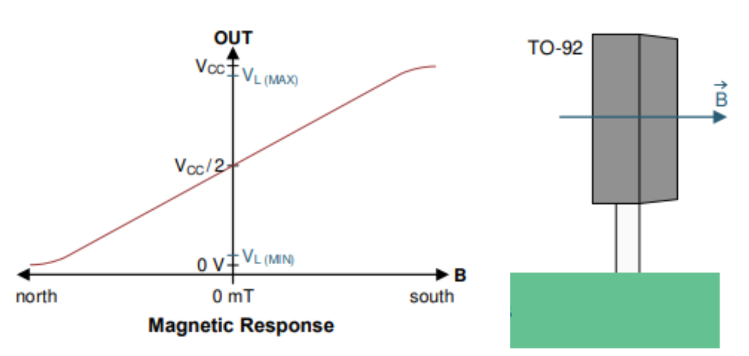
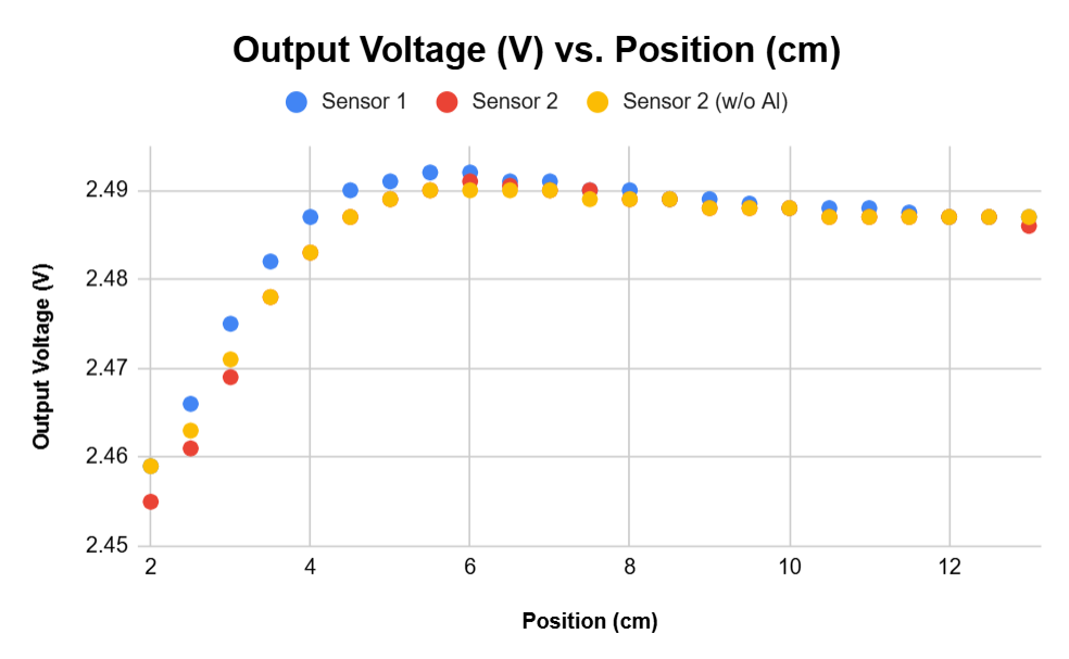
I experimentally characterized the sensors’ response to magnetic flux and used Taylor series approximation to define a function mapping each sensor’s output voltage to the magnet’s distance from it. I used this as the foundation of an algorithm that receives all sensor readings, identifies which sensor is closest to the magnet, and calculates the magnet’s distance from that particular sensor.
Read my Digikey Article, which goes into detail on my initial design process, sensor characterization procedure, and firmware algorithm.
I also implemented code to calibrate the sensors and zero out any constant magnetic flux from the environment, as well as inherent manufacturing offsets between individual sensors.
Motherboard for Autonomous Oceanic Drone
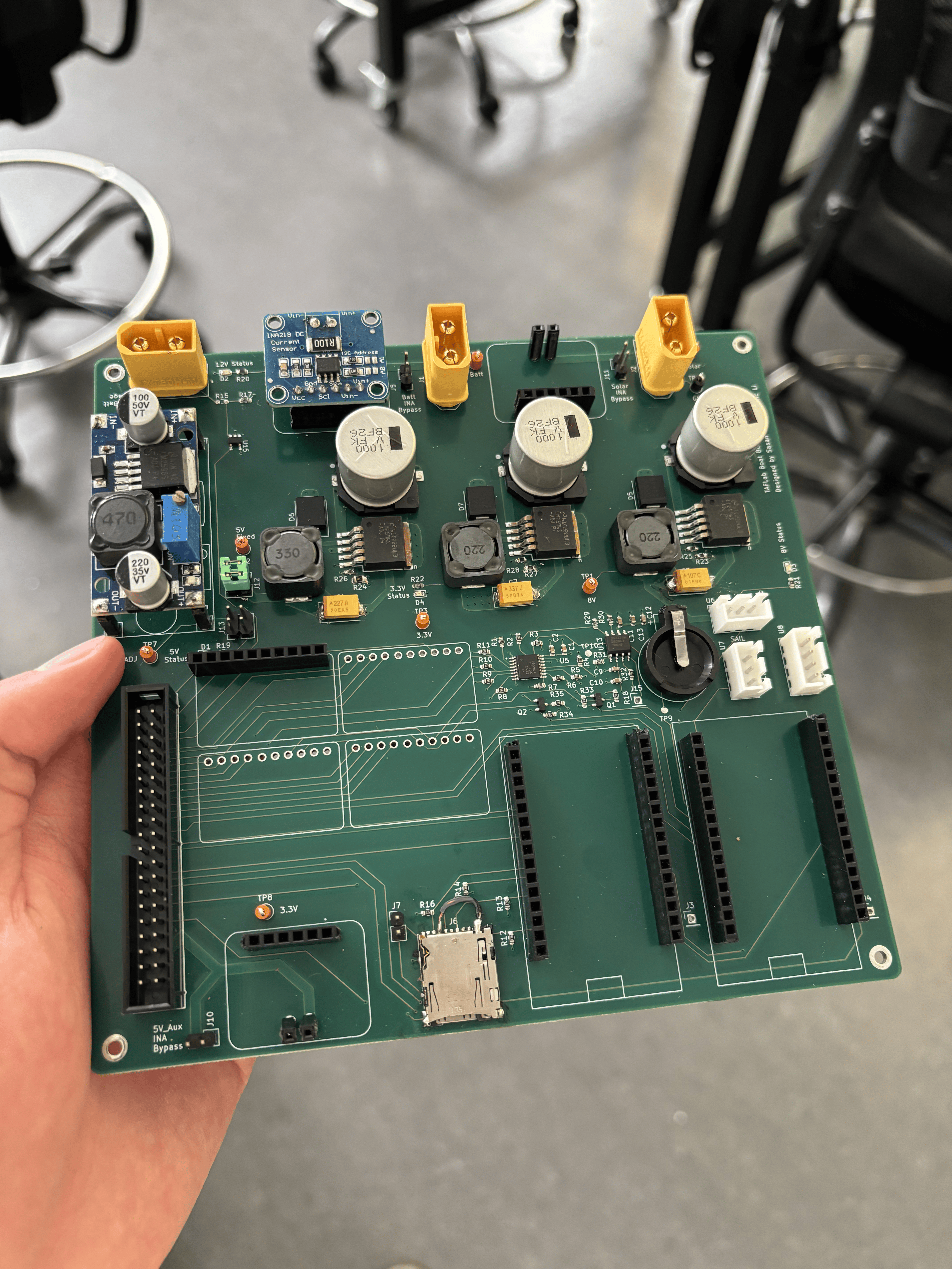
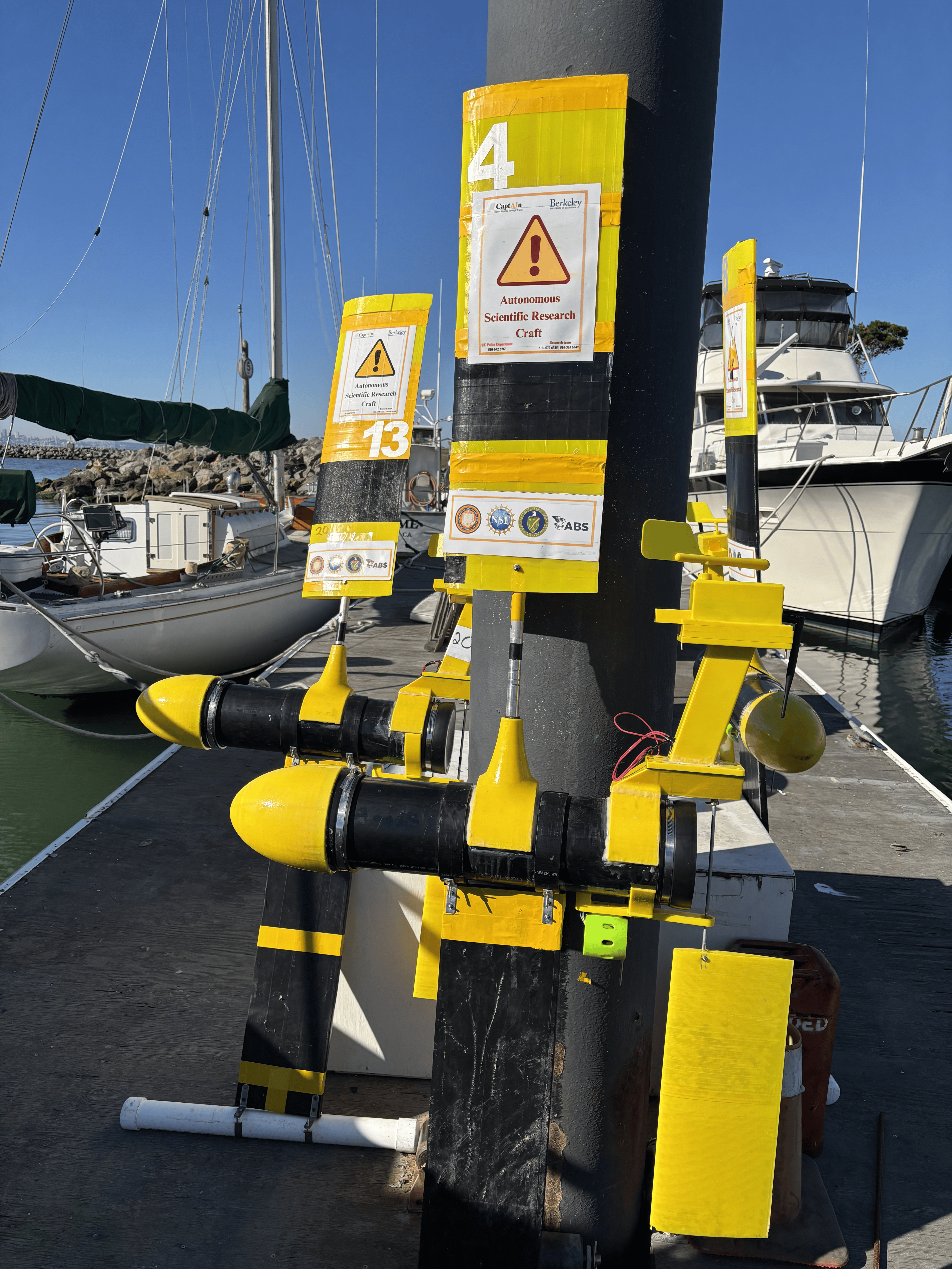
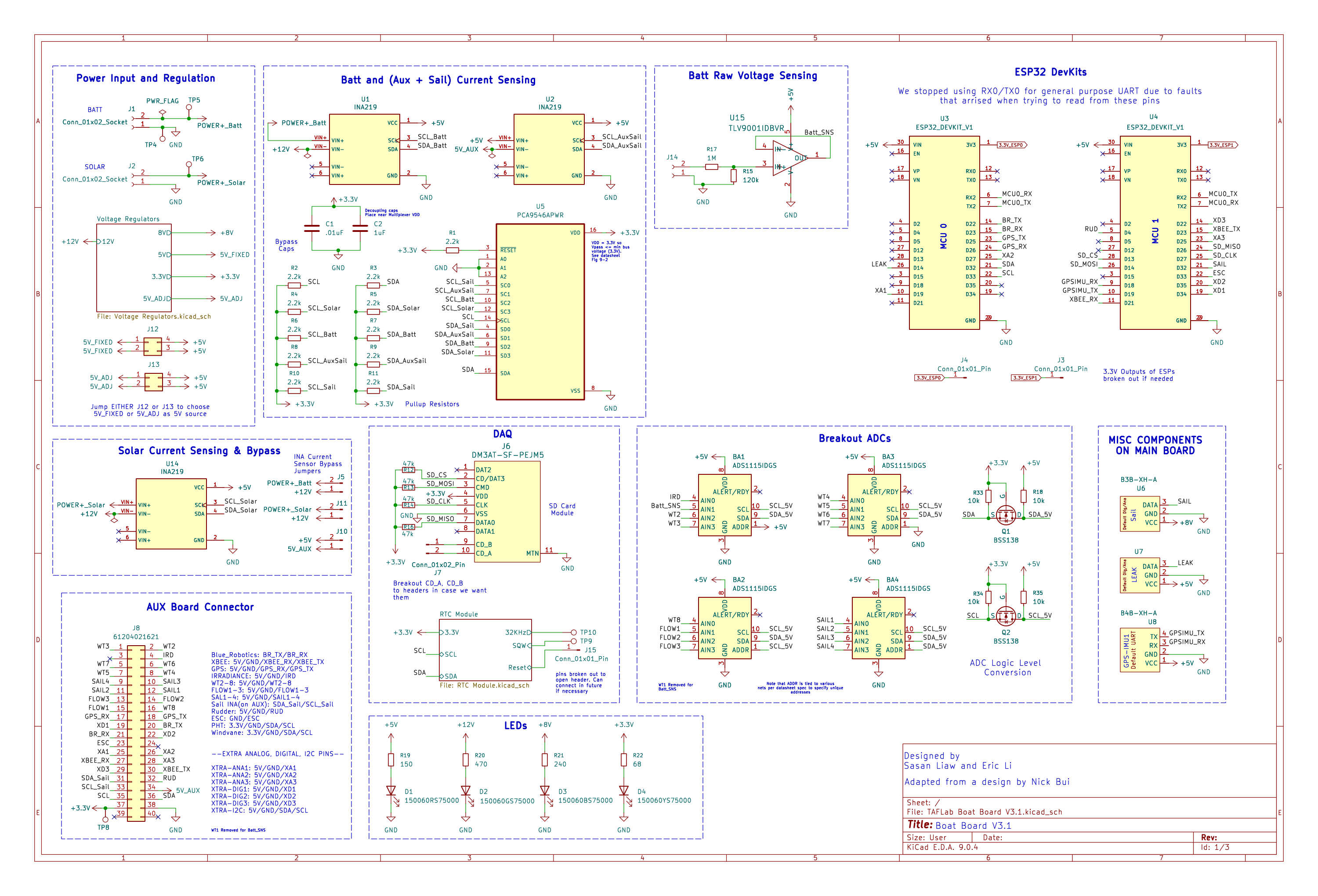
For this project, I collaborated on the complete redesign of the motherboard for an autonomous oceanic drone designed to monitor temperature and other environmental factors over extended deployments. While a fellow researcher and I co-designed the schematic, I took sole ownership of the PCB layout.
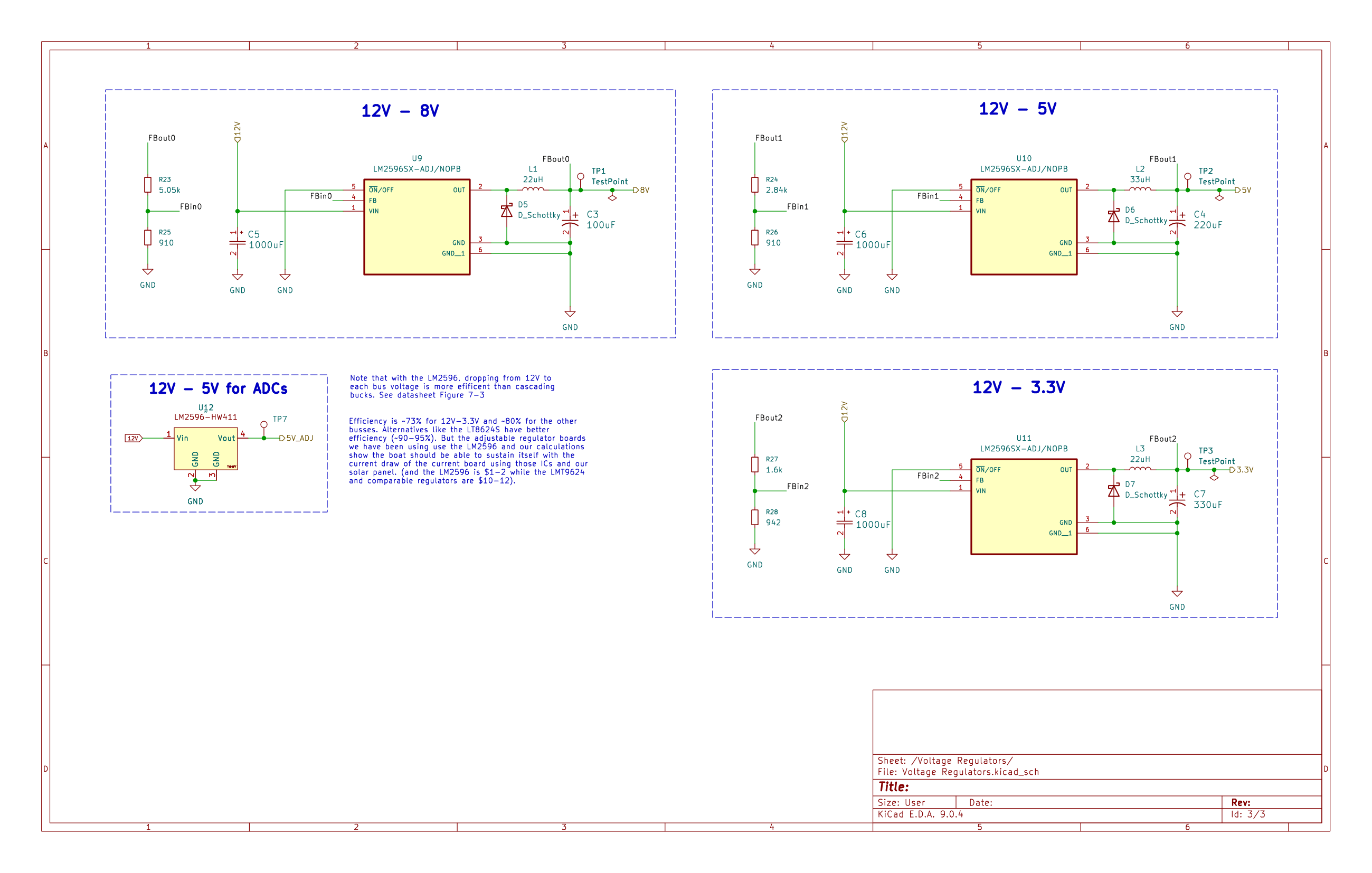
This work was done during my time in the Theoretical and Applied Fluid Dynamics Laboratory (TAFLab) at UC Berkeley.
I was responsible for integrating multiple current sensing modules into the board to measure power draw from both an external lithium-ion battery and a solar panel. I selected a multiplexer to resolve I2C address conflicts between identical components and route their signals to the MCU.
I also selected appropriately sized inductors, feedback resistors, and input/output capacitors to use with the LM2596SX buck converter, regulating voltage down from 12 V to 8 V, 5 V, and 3.3 V. During layout, I minimized the size of switching loops, ensured low-impedance paths to stable power and ground rails, and kept the feedback path clear of any noisy nets. Utilizing large copper pours, power planes, and thick traces, I distributed this stable power throughout the PCB, accounting for potential spikes in current draw.
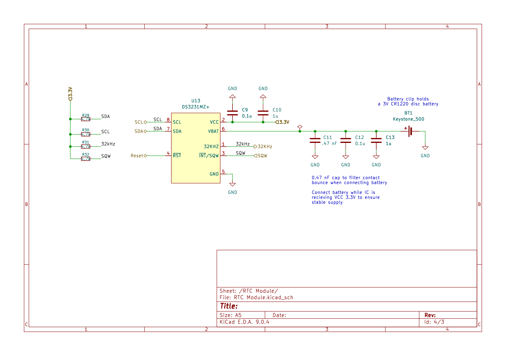
Additionally, I integrated a microSD card receptacle for data acquisition and connected it to a real-time clock (RTC) module my partner designed. I also added circuitry to measure the voltage of a 40 V battery (before it is dropped to 12 V by an external regulator for the board’s main supply), using a large resistor divider and op-amp buffer to feed it into a 5 V input ADC.
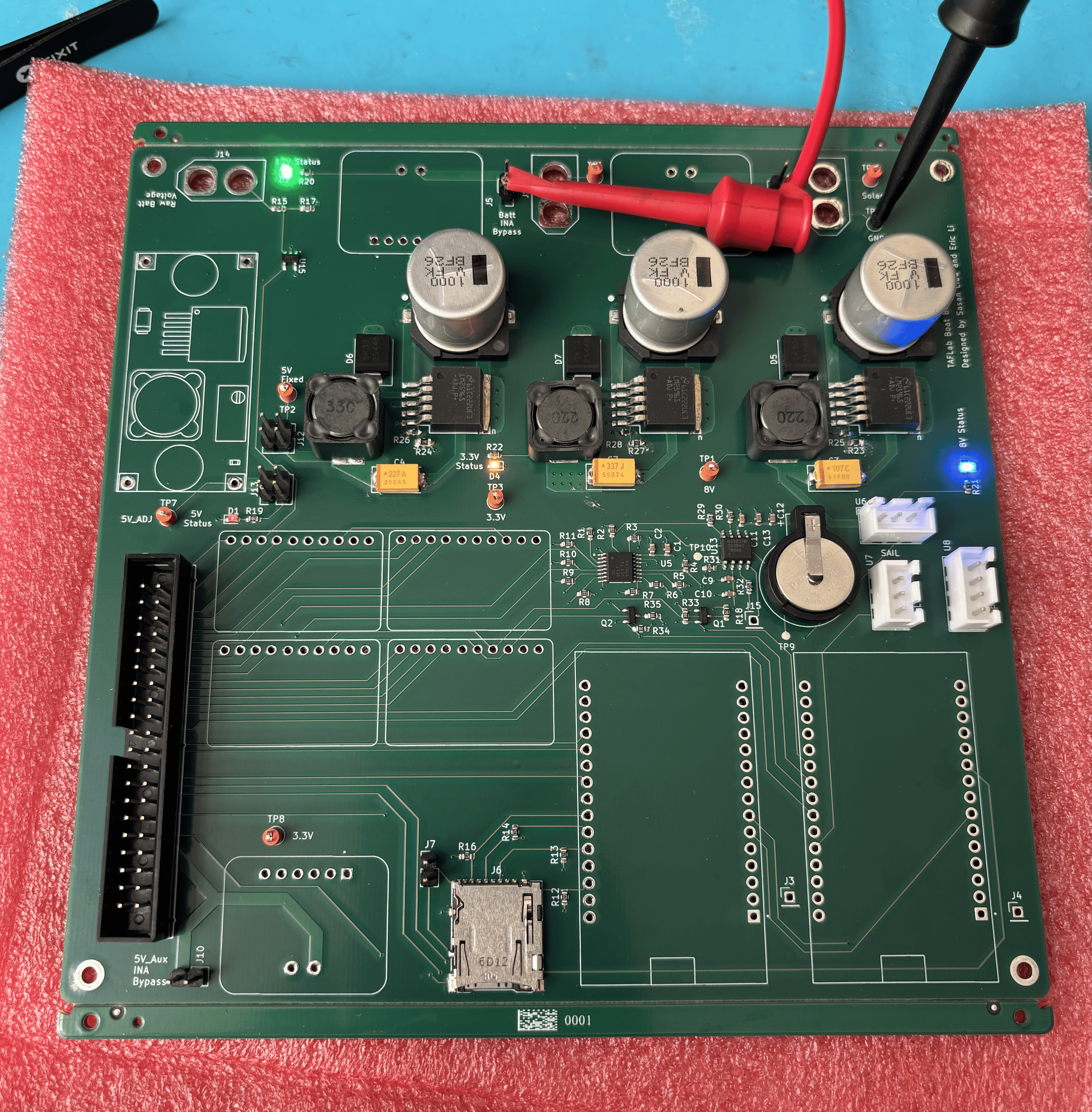
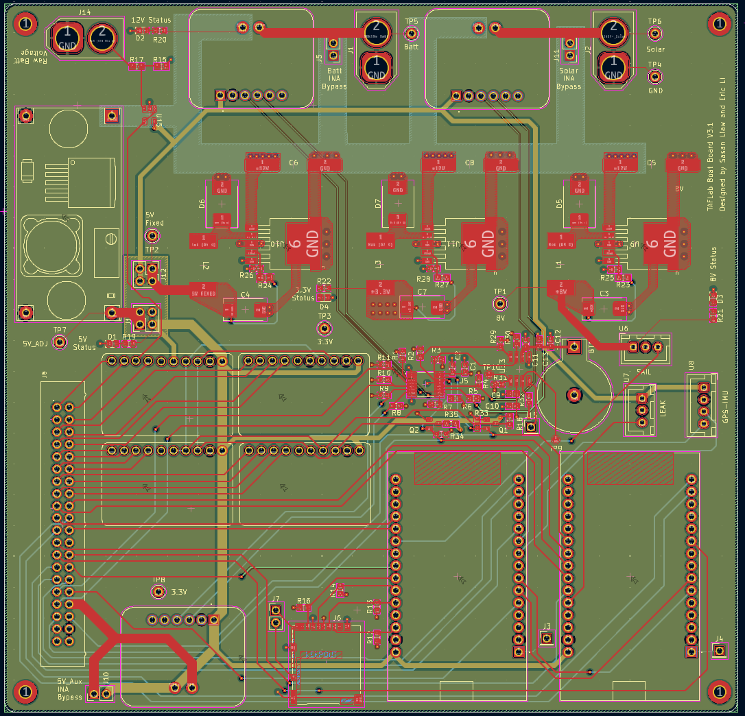
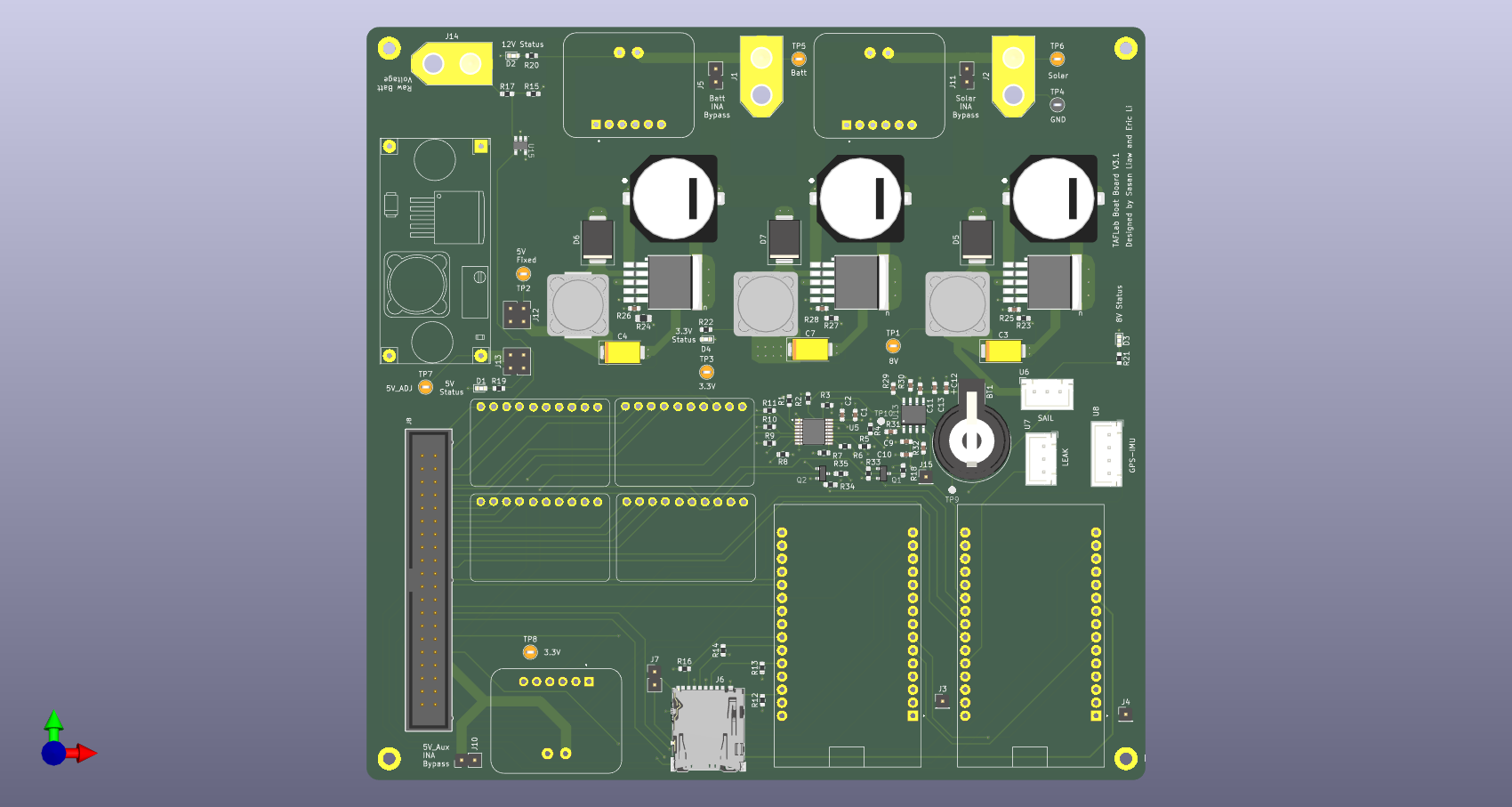
I strategically placed test points throughout the PCB for debugging, added indicator LEDs on each power rail, and placed pins to bypass the current sensors if necessary. I also added headers to enable source selection of the 5 V rail between the SMD buck converter and an off-the-shelf (OTS) adjustable regulator (that would regulate 12 V to ~5 V). The latter was included in case slight adjustments to the rail were needed to calibrate analog sensors using it as a reference.
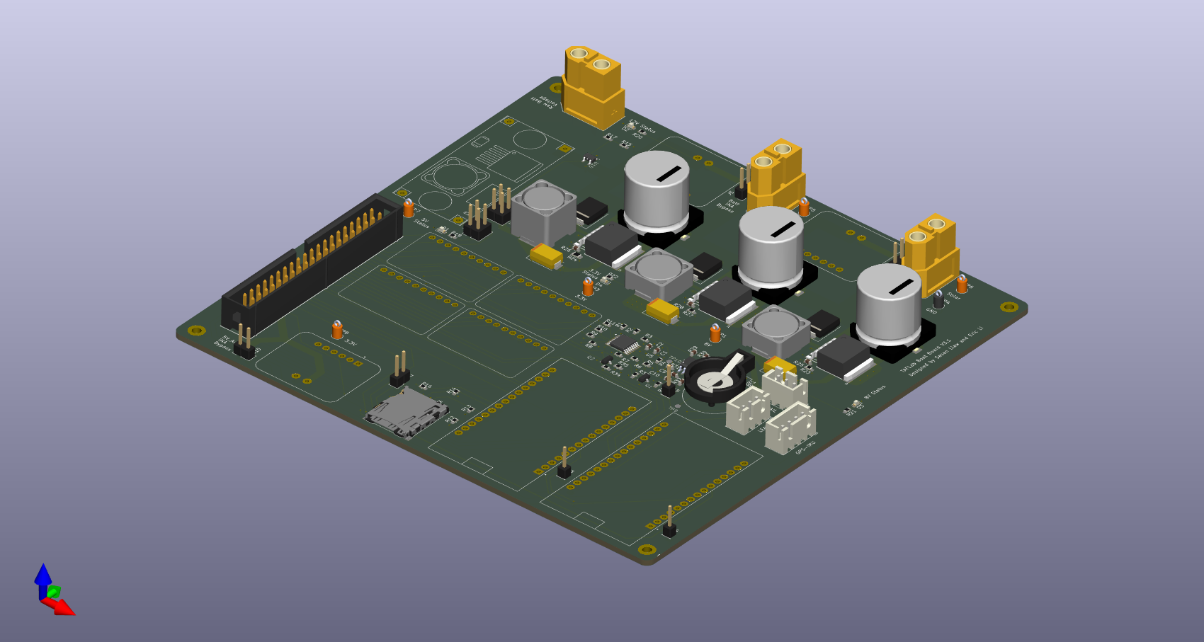
I made significant improvements in layout from the previous iterations of this board. The previous version used by this research lab included just two signal layers, no power planes, and distributed power through large auto-routed trace networks. It also included OTS modules for voltage regulation and data acquisition, which were unreliable, had to be purchased separately, and required manual tuning. In my revision, prior to implementing additional functionality and converting OTS modules into SMD components, I redid the stackup to include four layers instead of two for better power stability. I also minimized trace length and overlaps wherever possible to preserve signal integrity, and decreased the via count from 84 to 36.
Two Stage Display Driver Op Amp
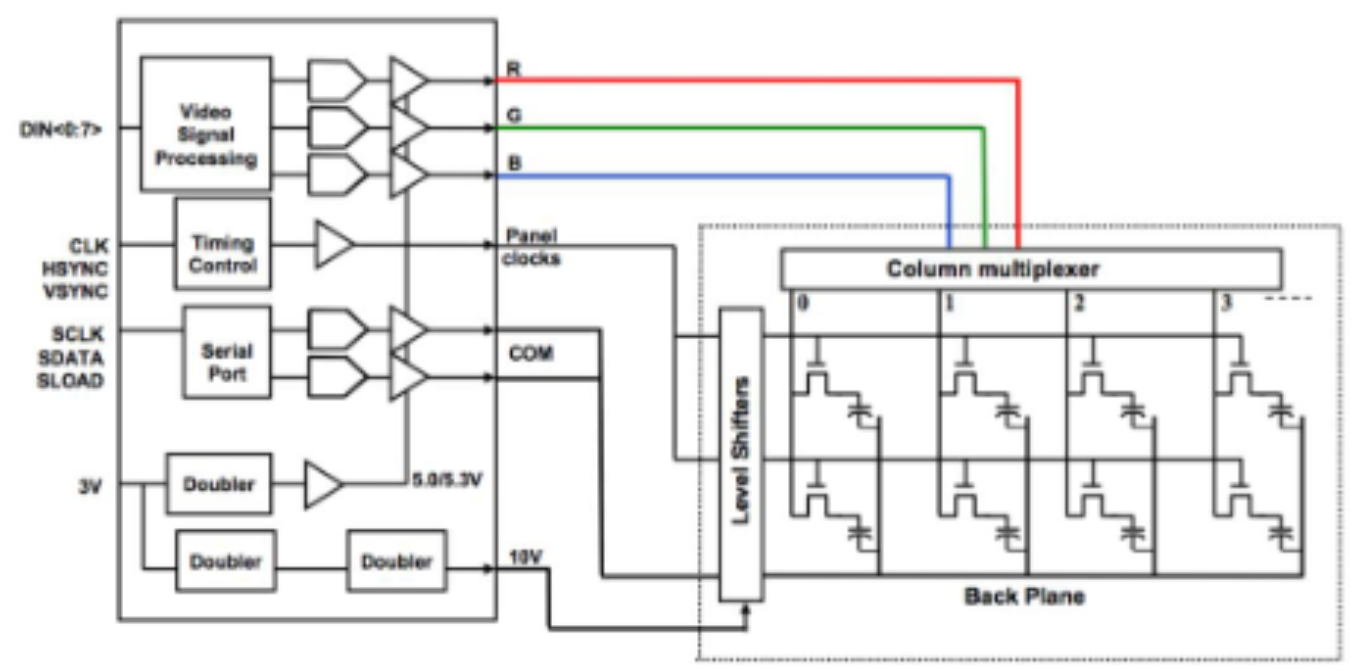
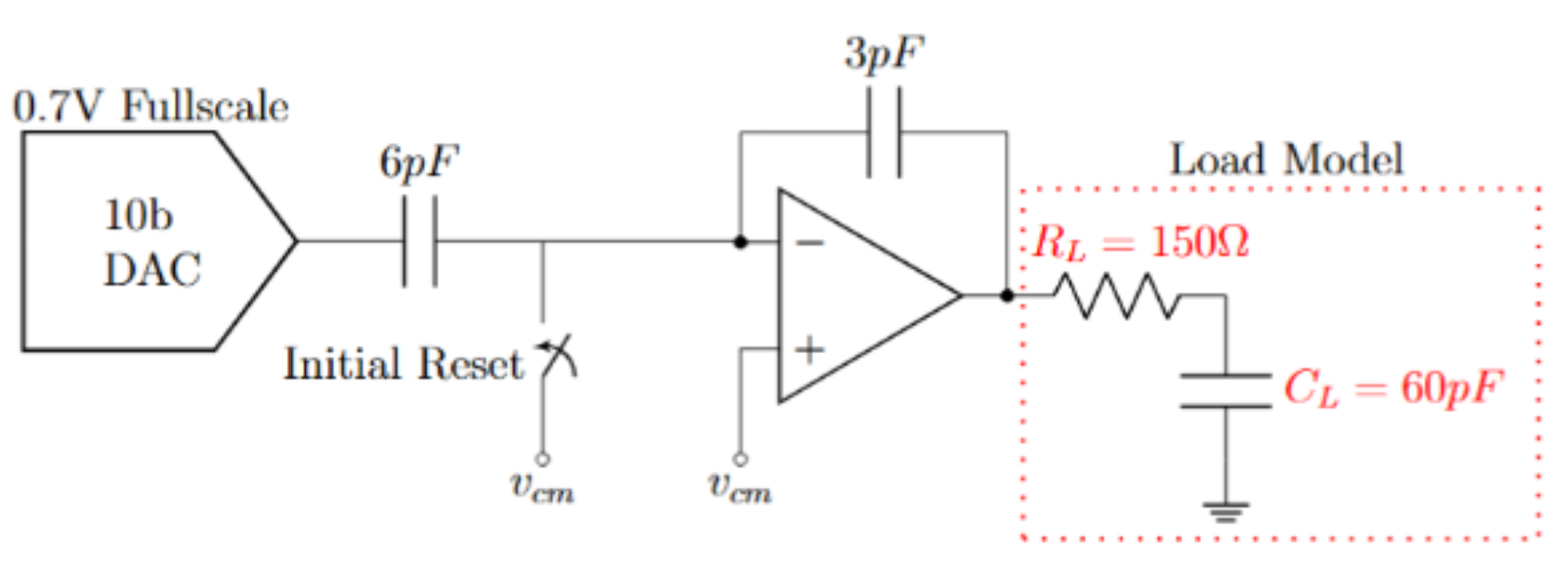
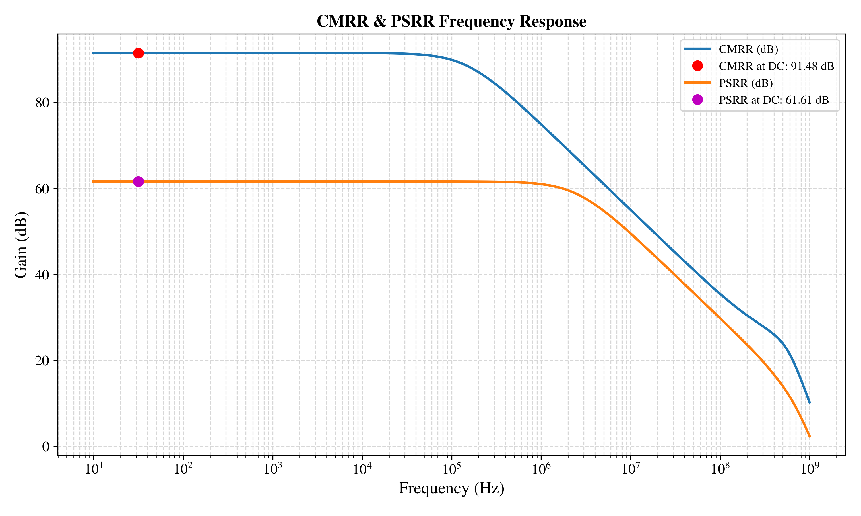
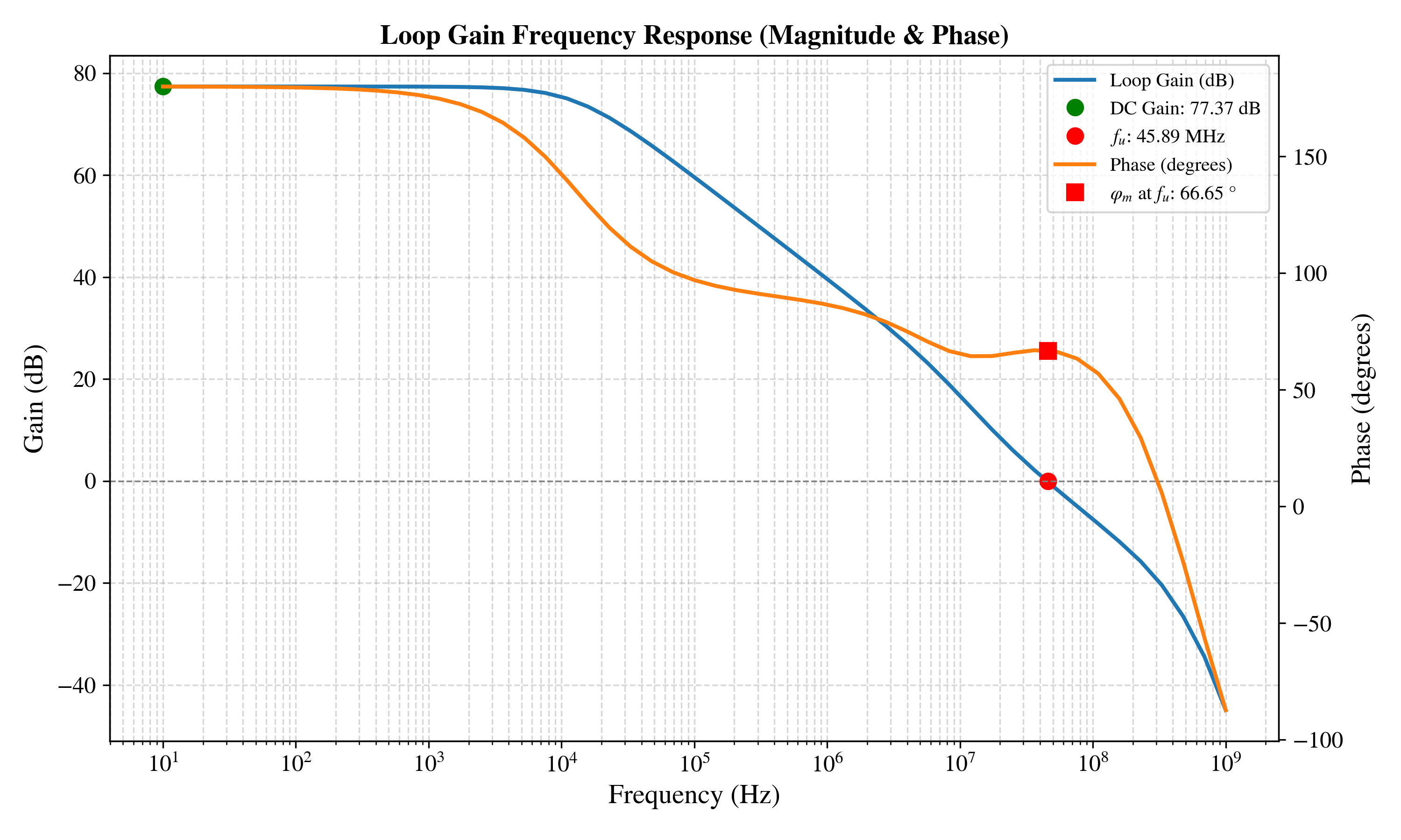
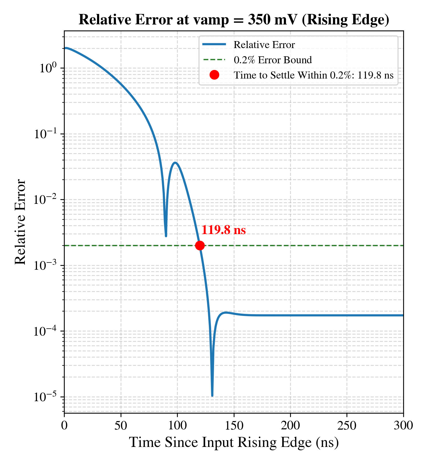
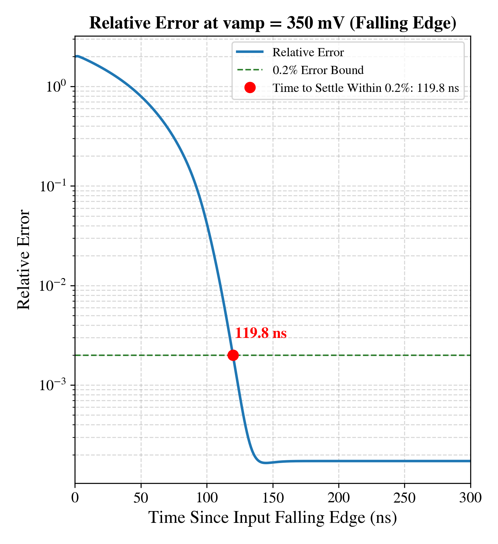
For this class project, I designed a custom operational amplifier capable of driving a 272 × 340 pixel display at 60 Hz. The amplifier needed to drive every pixel sequentially with ≤ 0.2% error, deliver a high output swing of 1.4 V, and be built at the transistor level with only a single current reference.
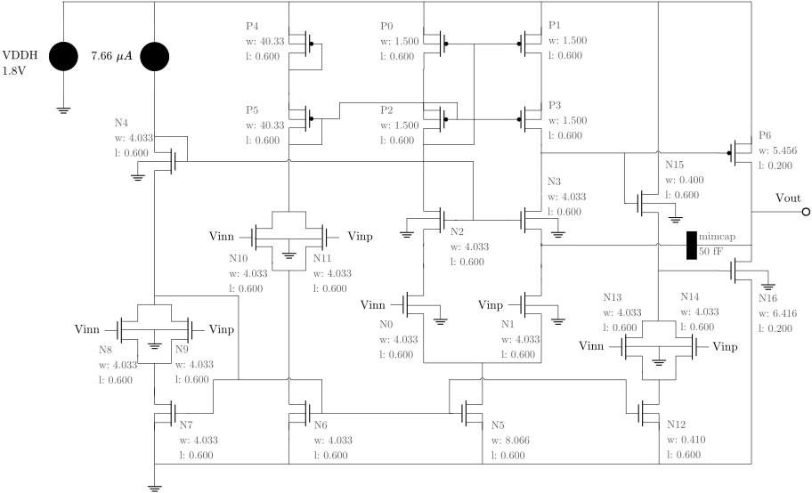
Read my full report which explains my design process, choices, and peformance results in detail.
Leveraging a two-stage architecture, I designed a telescopic differential input first stage to achieve high open-loop gain. Next, I implemented a Class AB common-source second stage to enable high output swing while minimizing power consumption. I utilized current mirrors to scale the current reference and distribute it to all branches.
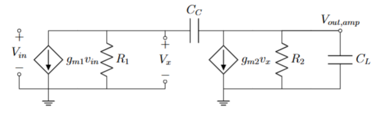
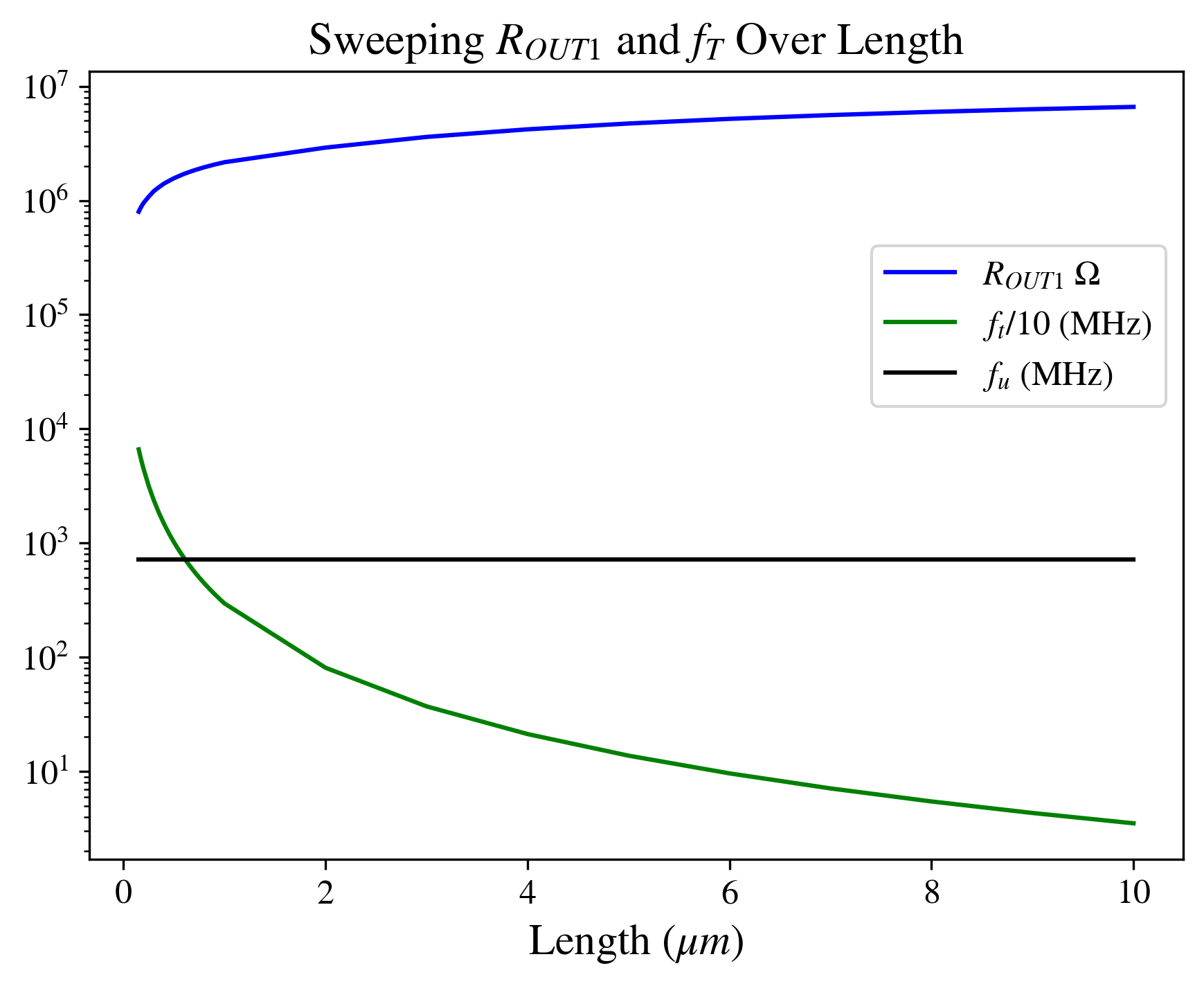
I began the design process with an idealized two-stage amplifier model and approximated the transconductance and output resistance each stage would require to achieve the desired specifications. I then wrote Python scripts to sweep data from lookup tables characterizing the selected transistors and calculated appropriate transistor sizing and DC bias points using the gm/Id methodology.
.png)
After generating these initial values, I built and simulated the full circuit in Cadence Virtuoso. I iteratively tuned the circuit parameters, accounting for parasitics and higher-order effects that were not captured in the initial model. I then validated that the final design met all specifications and documented the results.
Lithography on Oxides and Thin Films
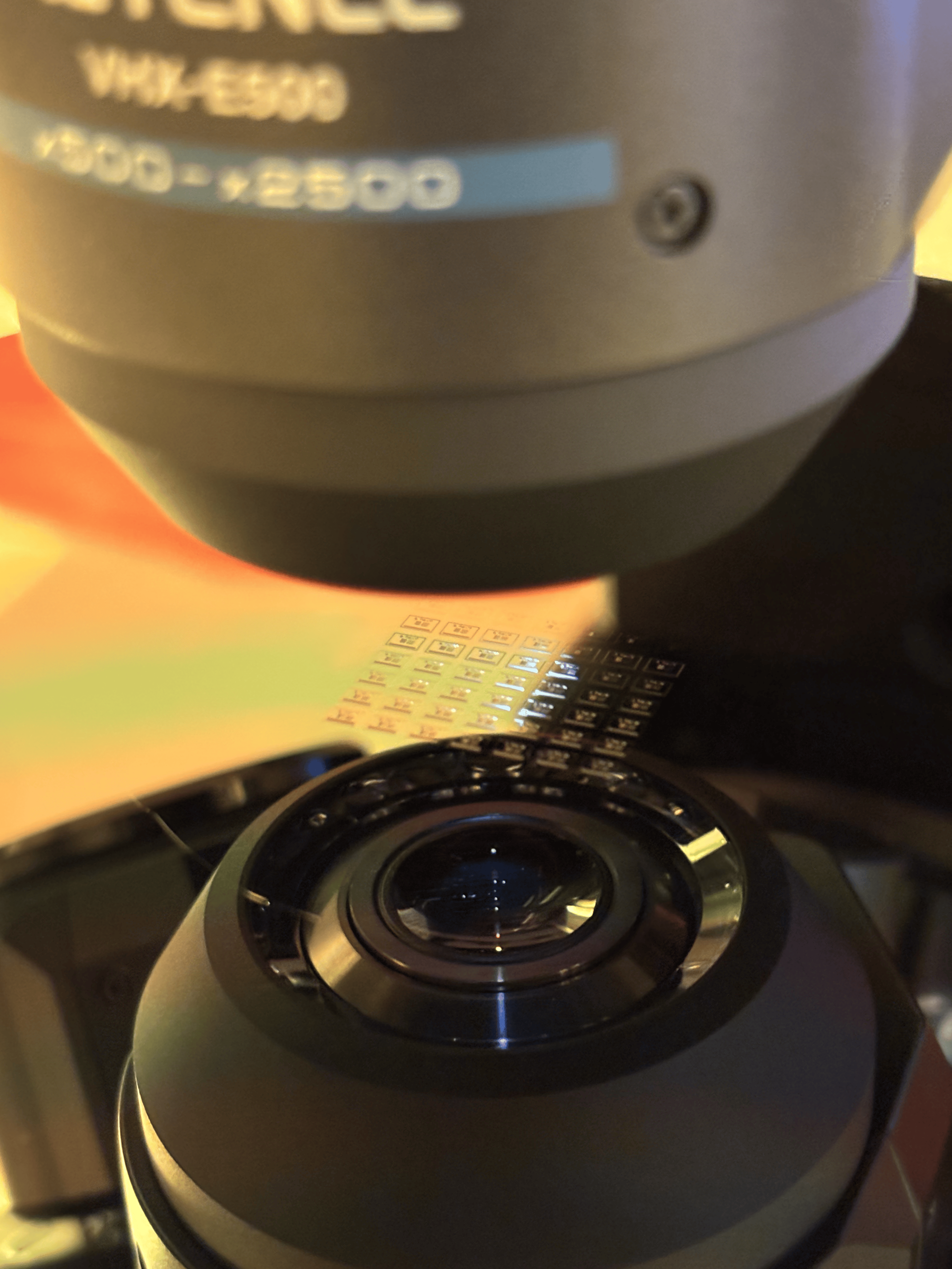
As a process engineering intern at the Marvell Nanofabrication Laboratory, UC Berkeley’s on-campus semiconductor manufacturing facility, I investigated how varying the material properties of the target surface affects optimal photolithography parameters. I then published these findings to guide process development for researchers and industry professionals using the facility’s tools.
Beginning with a literature review, I read currently available resources on lithography, dose-to-clear, reflection coefficients, and the absorption of materials that are commonly patterned in wafer-scale fabrication.
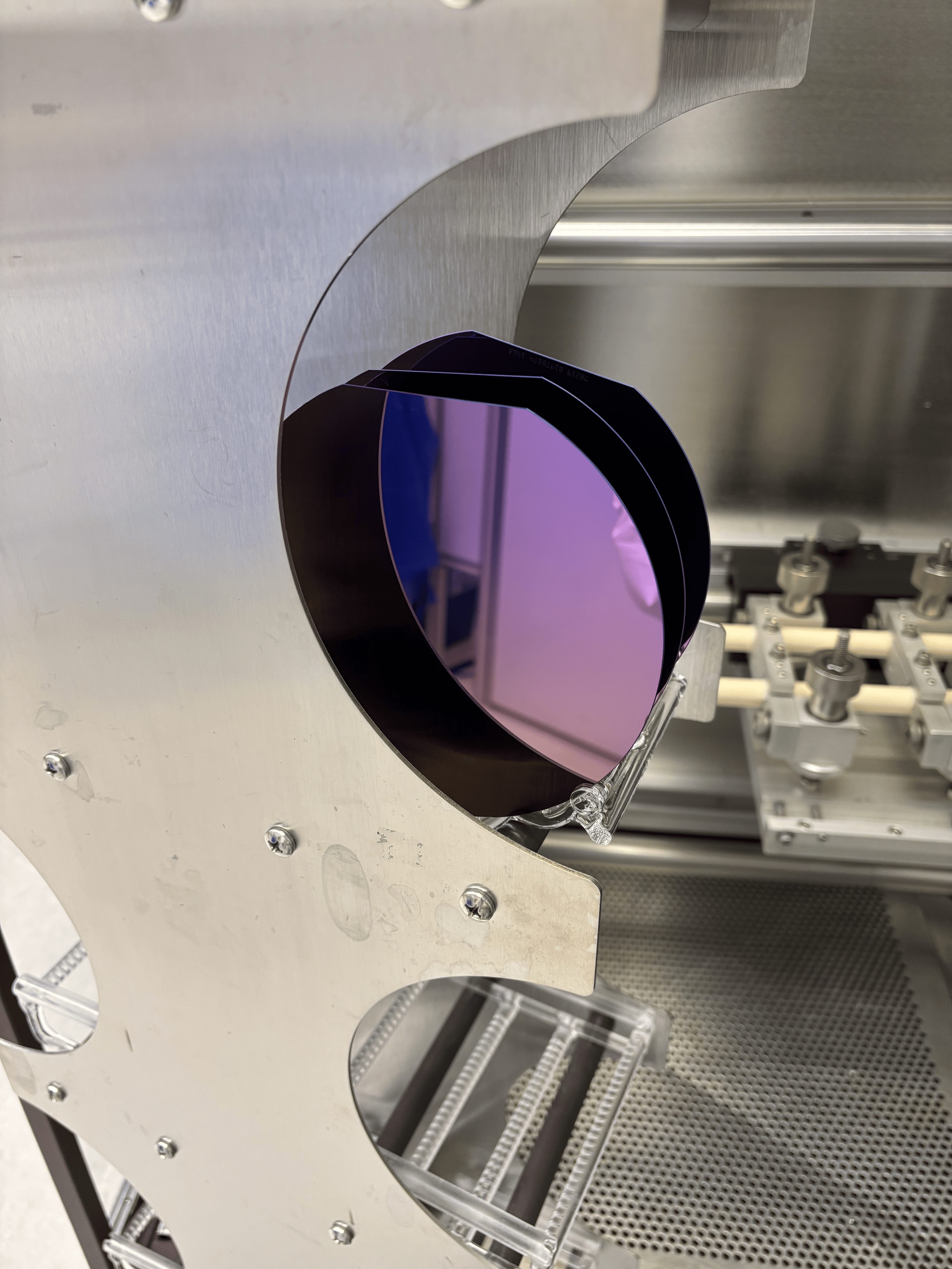
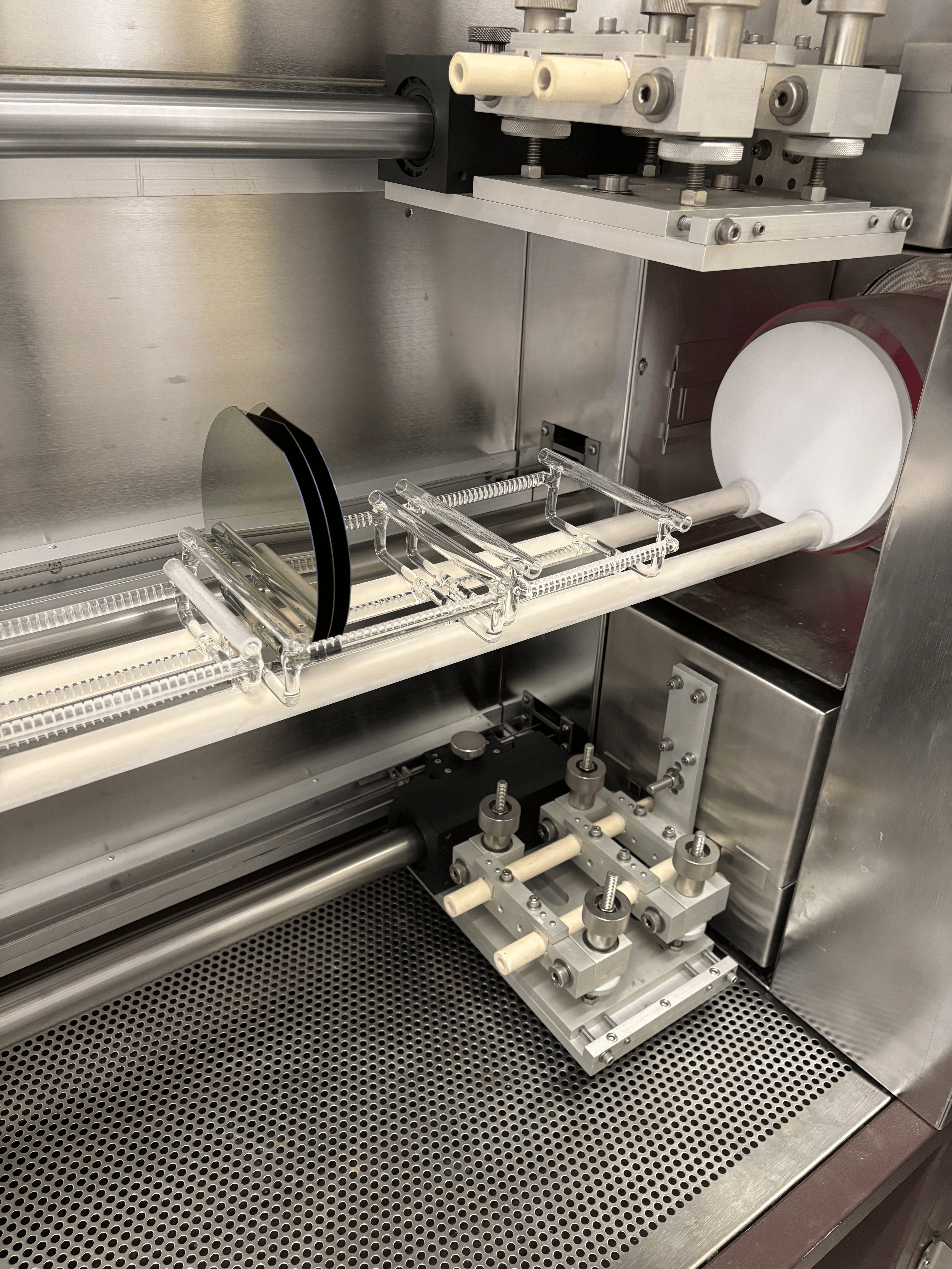
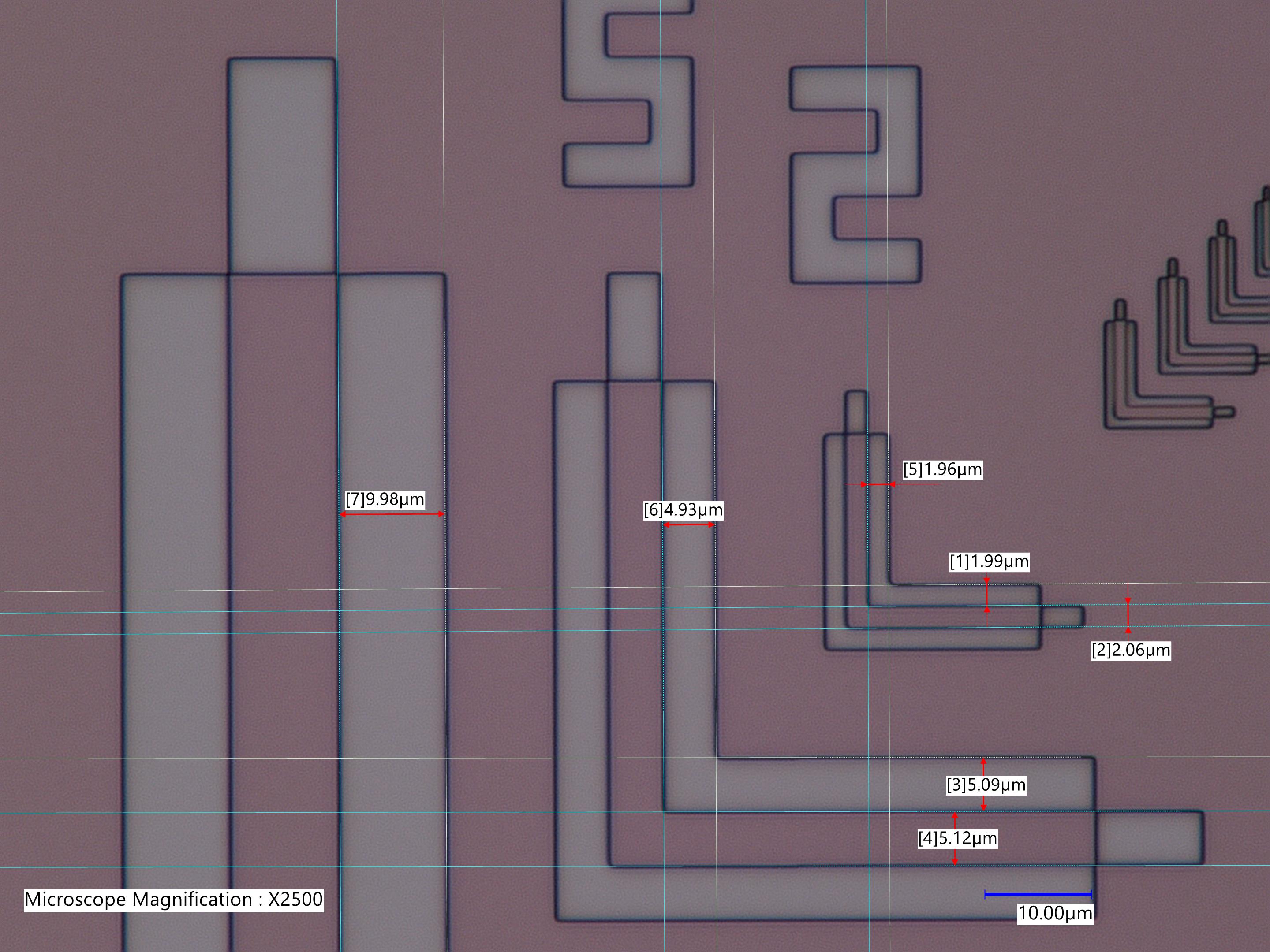
To test my theoretical predictions, I then grew SiO2 on cleaned bare silicon wafers using wet oxidation at 1000 °C. I did so at a variety of growth thicknesses: 1 kÅ, 3 kÅ, and 10 kÅ. I spin coated 1 μm of MiR701 i-line photoresist and used a maskless aligner exposure tool (Heidelberg MLA 150) to expose a test pattern across a range of doses (intensity in mJ) and defocus levels. Following development, I inspected the wafers under an optical microscope to identify the dose and defocus settings at which the best resolution was achieved.
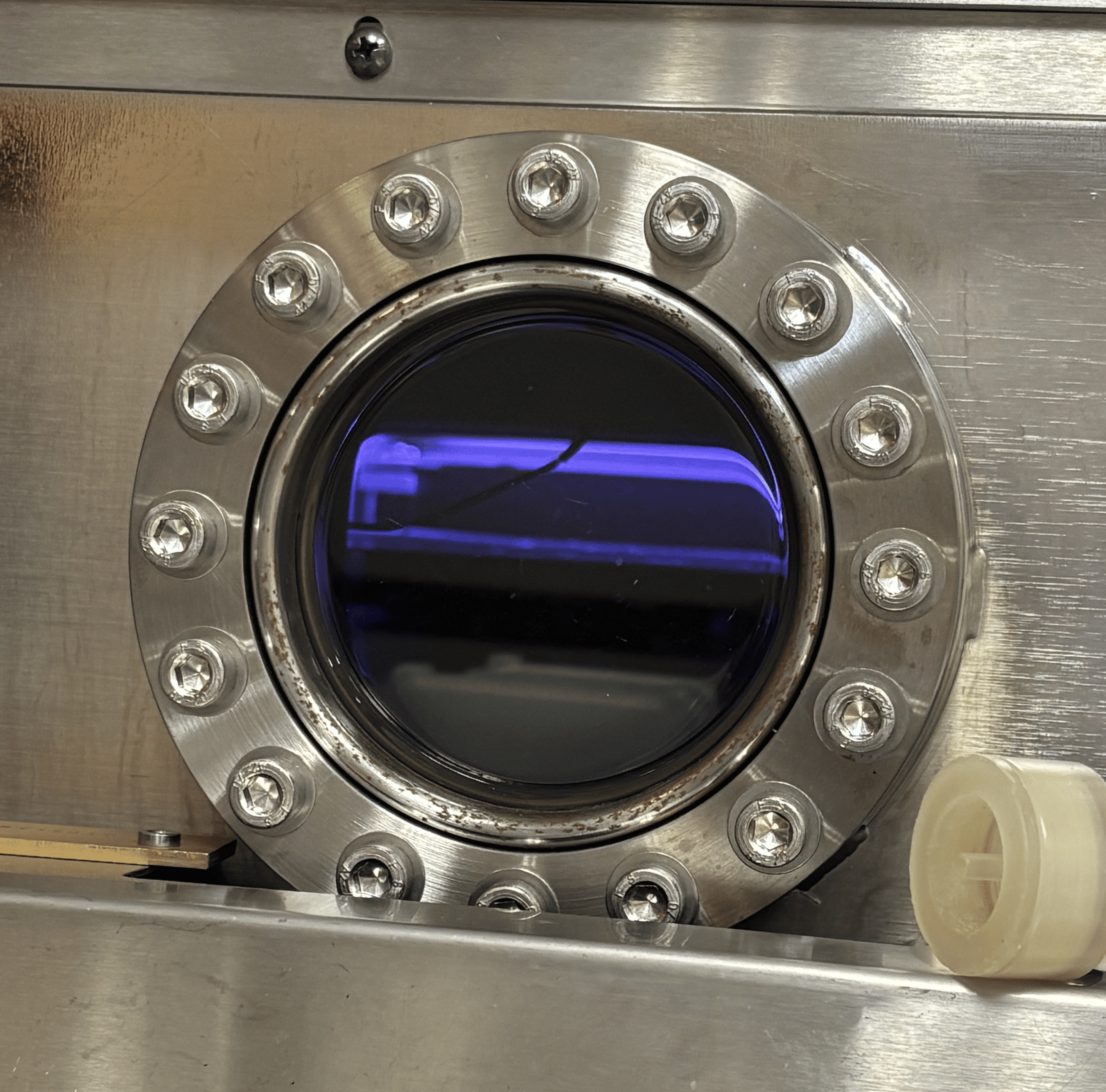
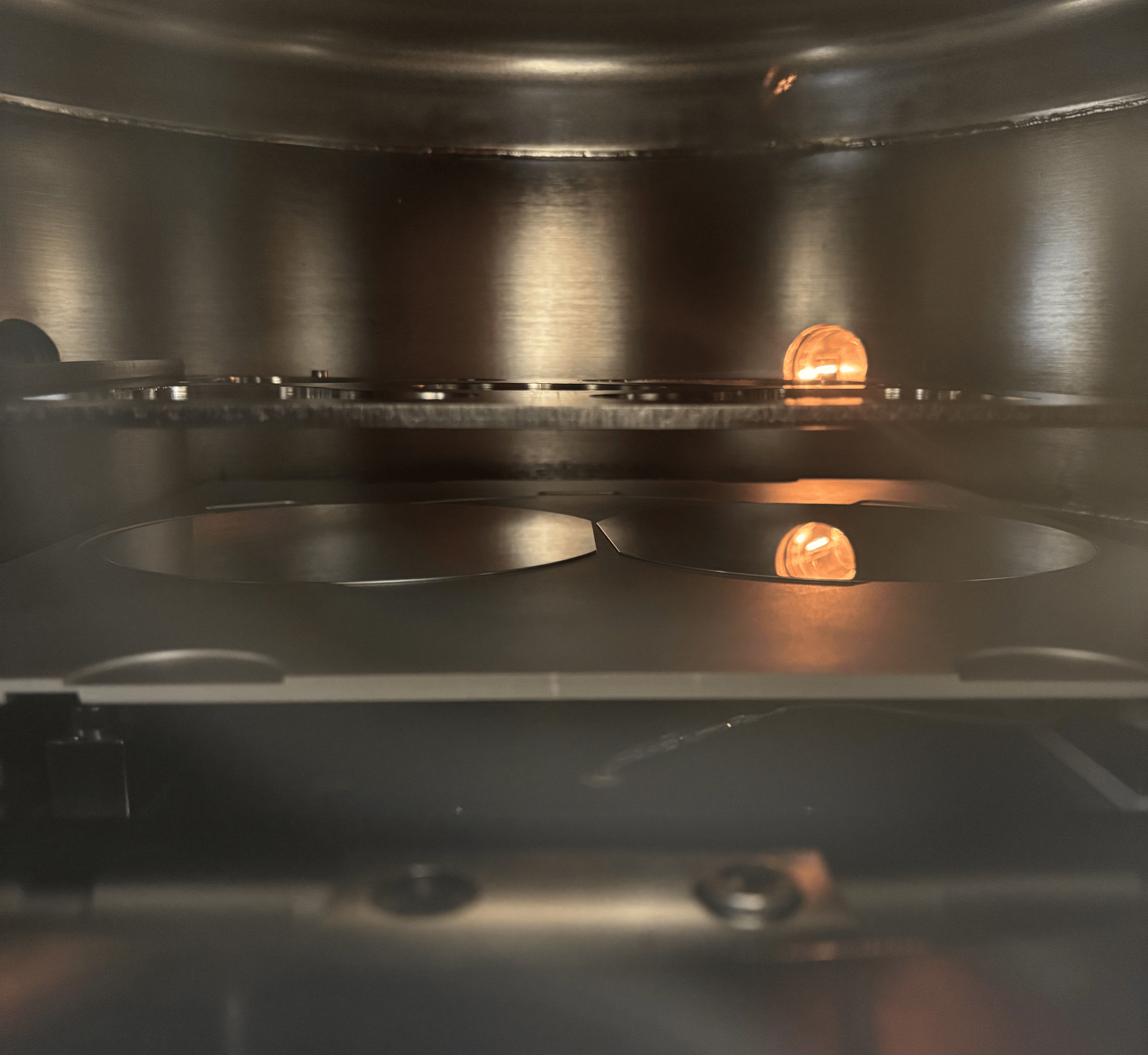
Next, I deposited thin metal films of aluminum, tungsten, and titanium onto new bare silicon wafers through both sputtering and electron beam evaporation processes. I performed photolithography on them in the same manner as with the SiO2 samples and documented the results.
As expected, the dose-to-clear of resist on SiO2 exhibited little deviation from lithography on bare silicon as the grown SiO2 layer was increased in thickness, since SiO2 has a very low absorption coefficient. The metal thin films had varying effects on lithography, requiring different dose adjustments depending on their reflective properties.
Read my write-up on my findings, now available on the Marvell Nanolab's website.
Treble Boost Circuit
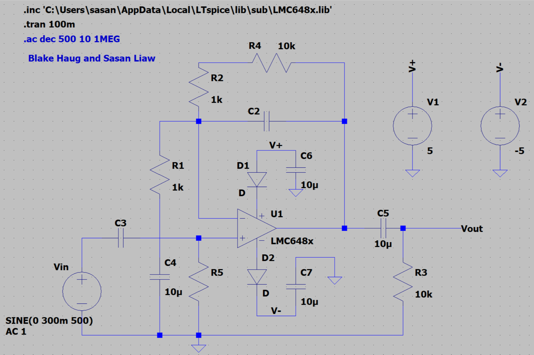
For this class project, I collaborated with a partner to design, construct, and test a bandpass circuit that receives input from an electric guitar and amplifies frequencies pleasant to the human ear, 300 Hz to 15 kHz, before outputting the signal to a speaker. We designed the filter to have a gain ≥ 10 within the desired band and minimal gain outside of it.
Given a circuit topology, we determined the symbolic frequency response of the circuit, identifying its gain, poles, and zeros in terms of unknown resistor and capacitor values. I derived the transfer function, factoring it into a gain term, a high-pass filter, and a pole-zero pair to easily identify the relationships between passive component values needed to achieve gain and cutoff frequency specifications.
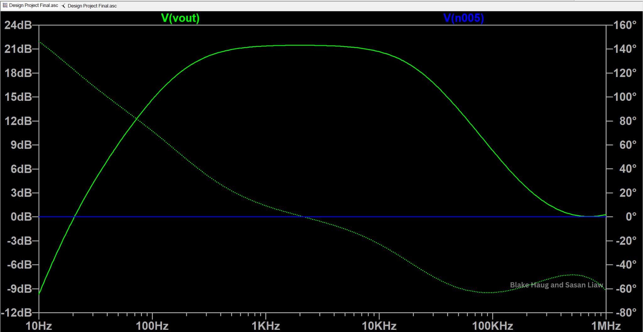
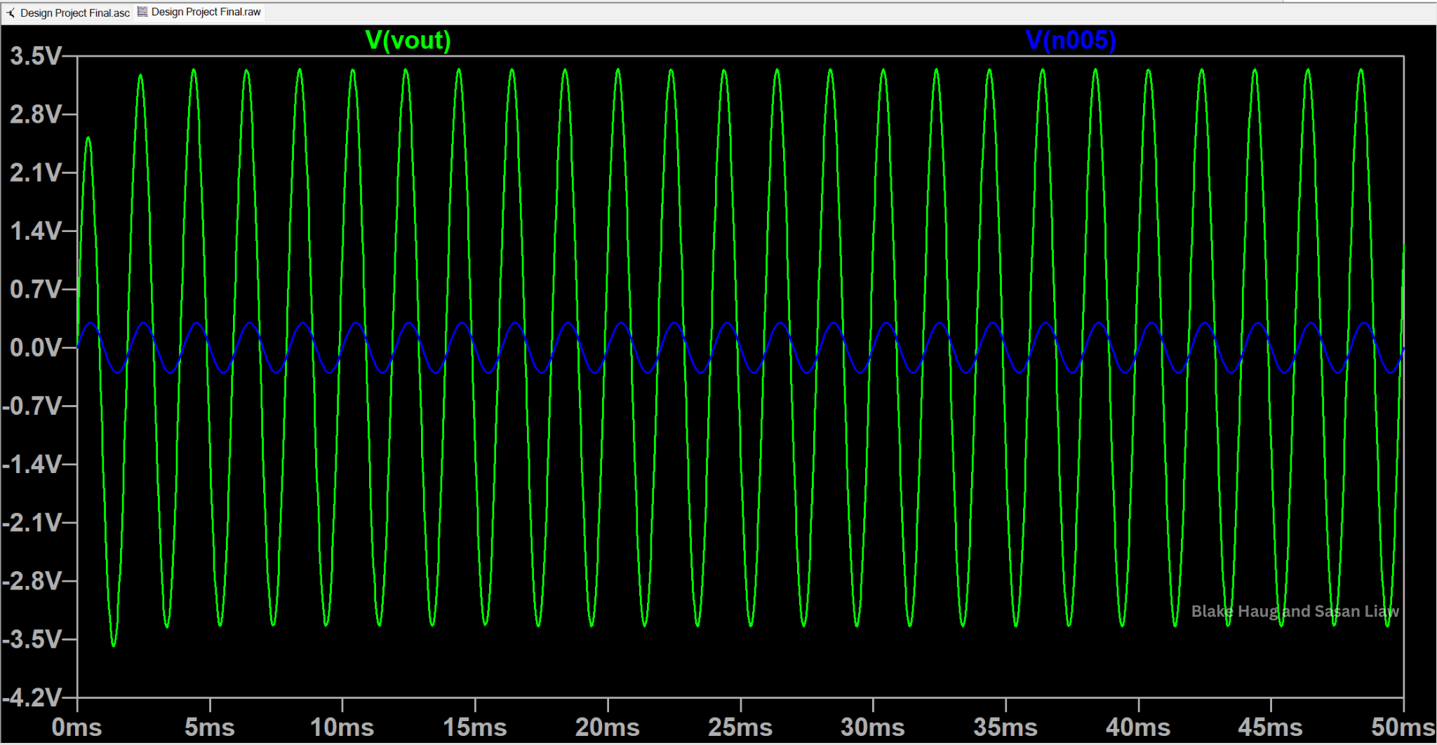
I then worked with my partner to determine these values and simulate the circuit in LTspice to verify it met specifications. We analyzed both its frequency response from 10 Hz to 1 MHz and transient response at a frequency within the passband (500 Hz).
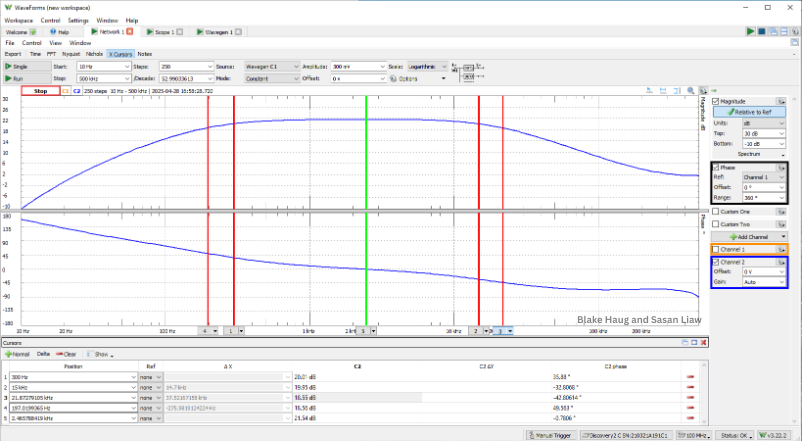
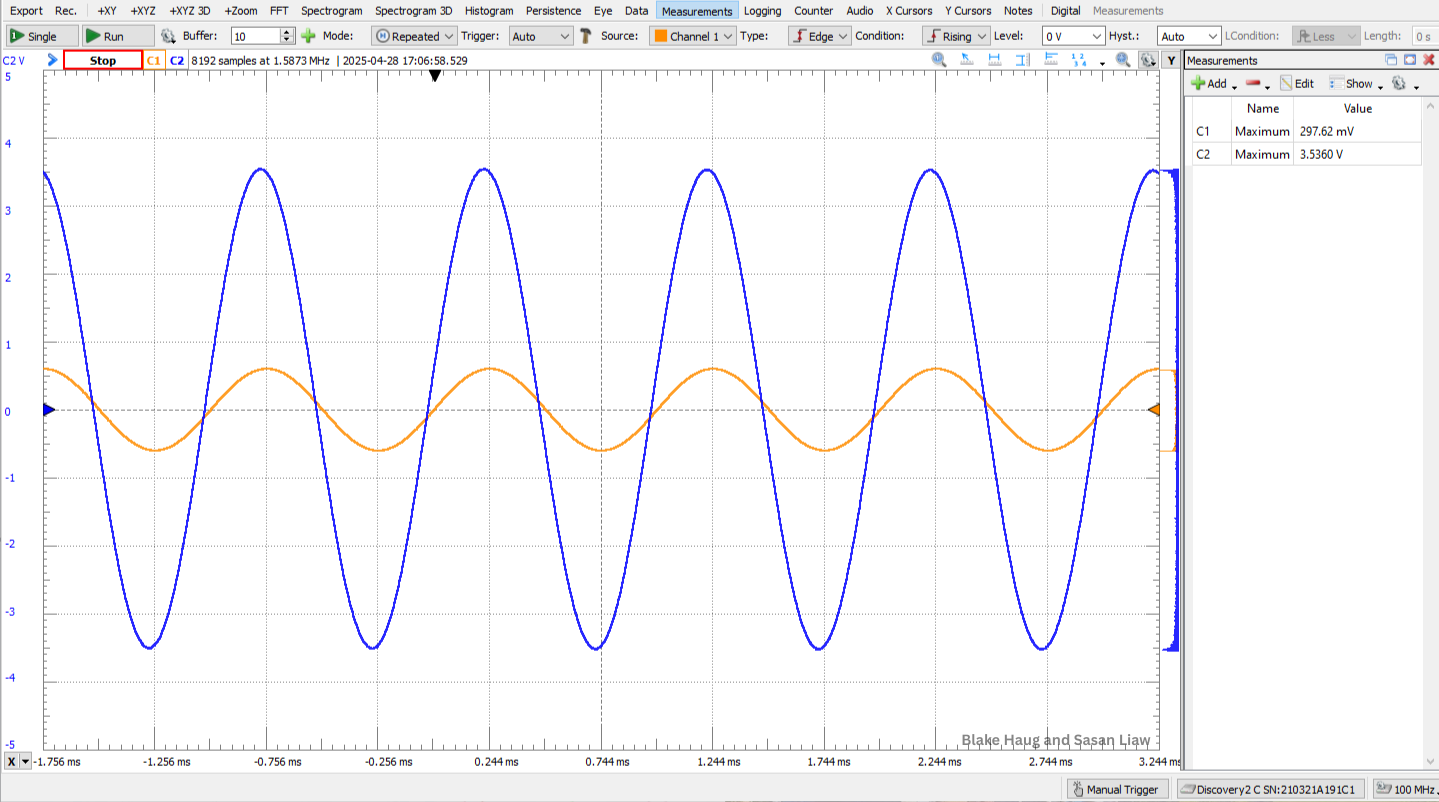
Finally, after proving the performance of the circuit in simulation, we built it physically using the LMC648 operational amplifier. Performing a frequency sweep, we validated that the circuit amplified frequencies within the specified band and not frequencies above or below it, achieving a midband gain of 21.58 dB, a lower -3 dB cutoff frequency of 197 Hz, and an upper -3 dB cutoff frequency of 21.8 kHz.
Photosensitive Alarm Clock
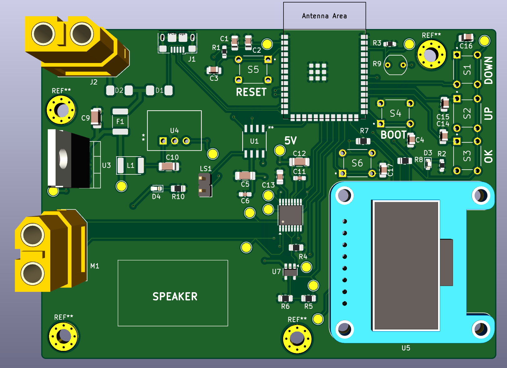
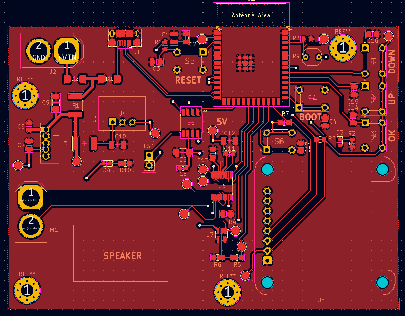
In this project, I collaborated with three teammates to engineer a custom alarm clock that automatically opens window blinds at dawn. The design included a photoresistor to detect changes in light intensity, a motor driver connected to a servo, an ESP32-S3 microcontroller, a screen, and a speaker with a corresponding amplifier.
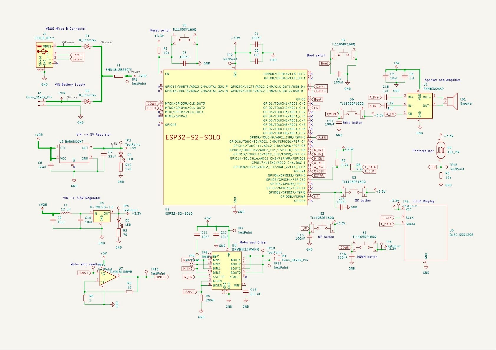
Together, we selected appropriate components while keeping the bill of materials (BOM) under $50, designed the PCB, and tested it. We completed schematic capture and layout in KiCad.
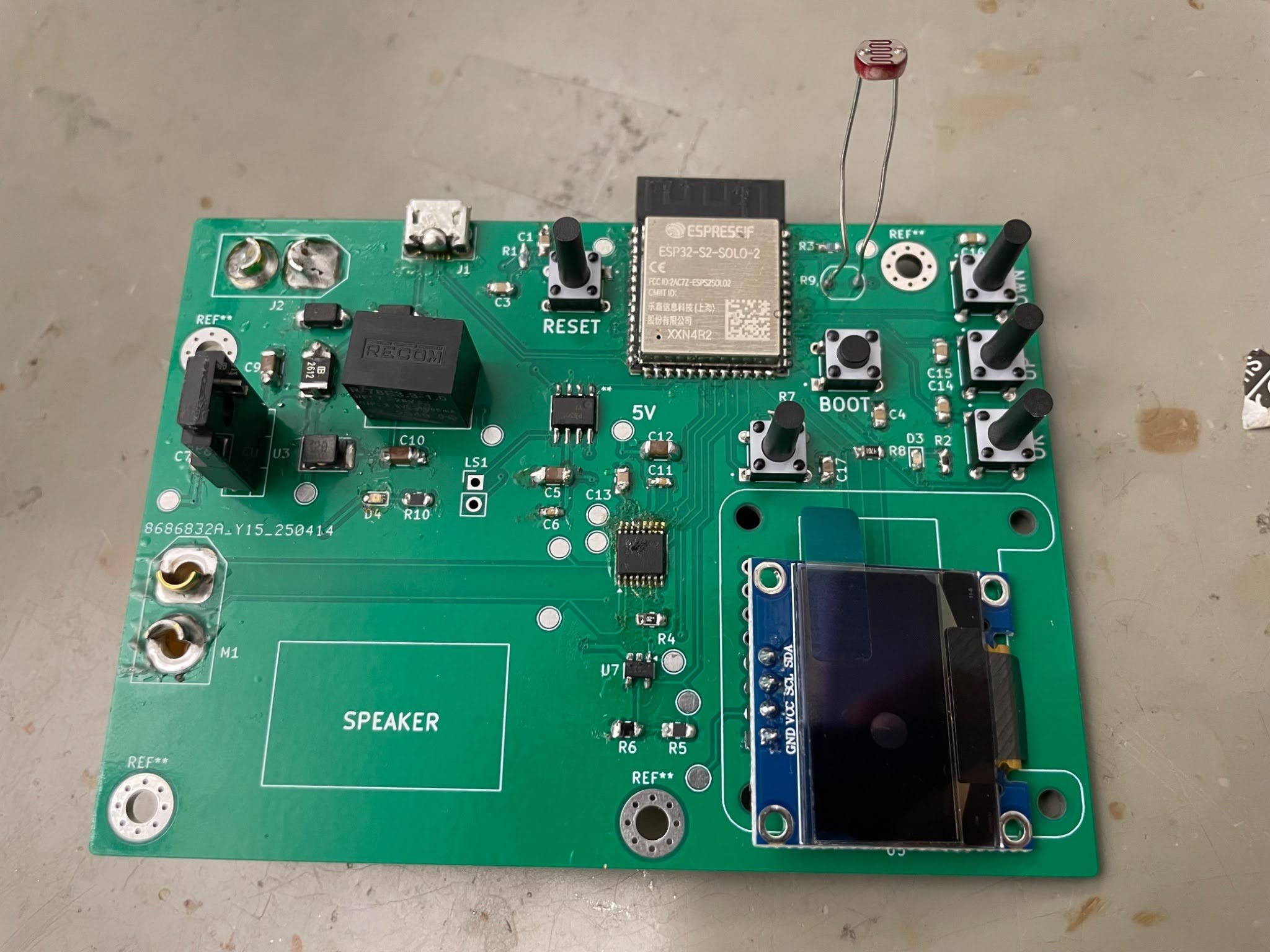
During assembly, the micro USB receptacle needed to flash code to the microcontroller (MCU) was ripped off the board along with some pads. We bypassed the damaged footprint by directly soldering the microcontroller pads to an MCU breakout board with its own USB receptacle, restoring the ability to upload code. While this pushed development back and we were unable to finalize functionality in the screen and speaker, we successfully implemented the photoresistor and servo by the project deadline.
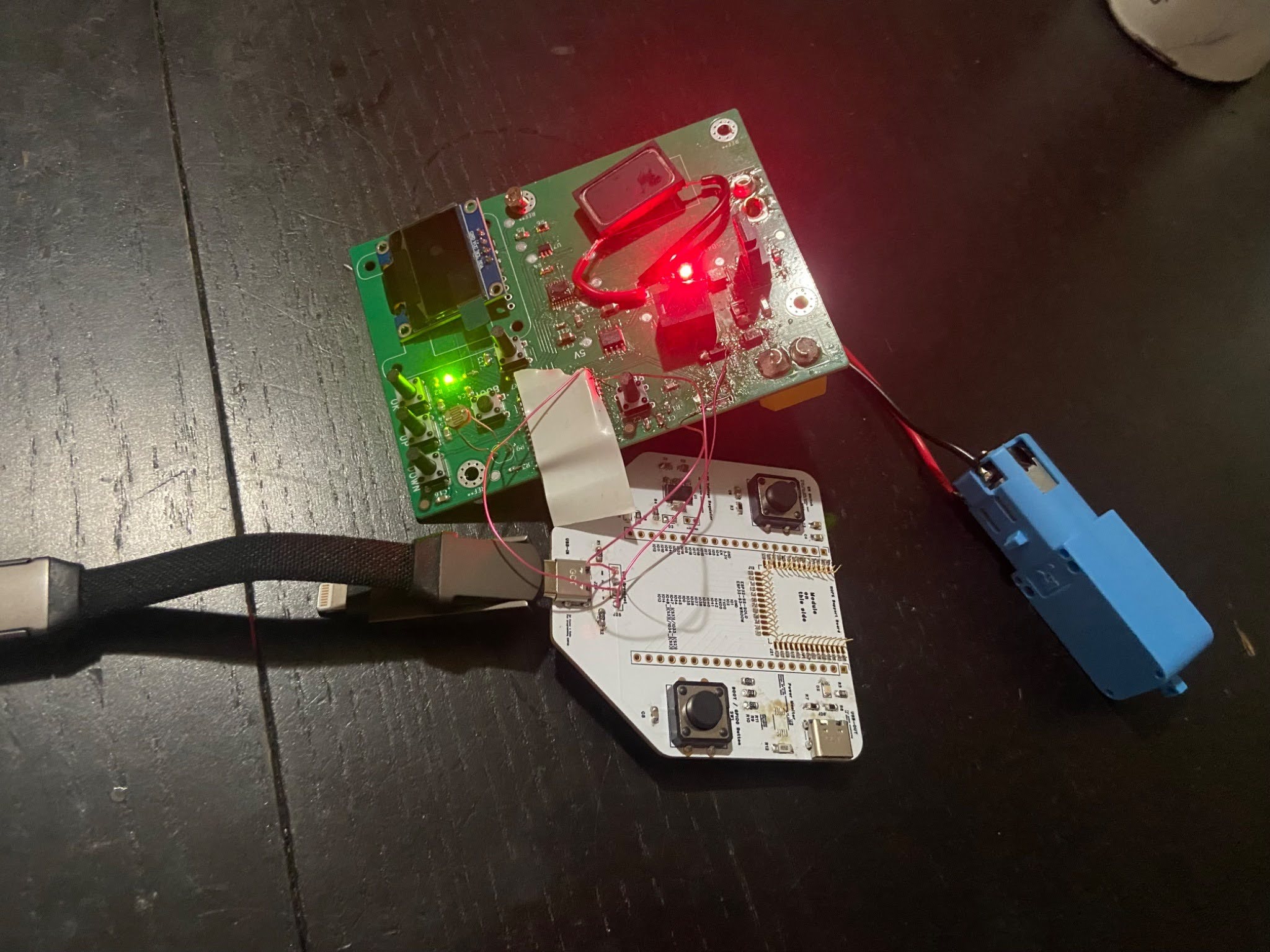
I wrote control logic using the Arduino framework to actuate the servo upon sensing changes in light intensity. We successfully demonstrated this functionality during the final review of the board. The photoresistor’s resistance would vary in response to light and, by using this as one half of a voltage divider, we read a change in voltage and passed it into the MCU’s built-in ADC.
3D Printing

Command Strip Shelf
Easy-to-install and easy-to-remove shelf for small items and decorations. Uses Command Strips.
View on:
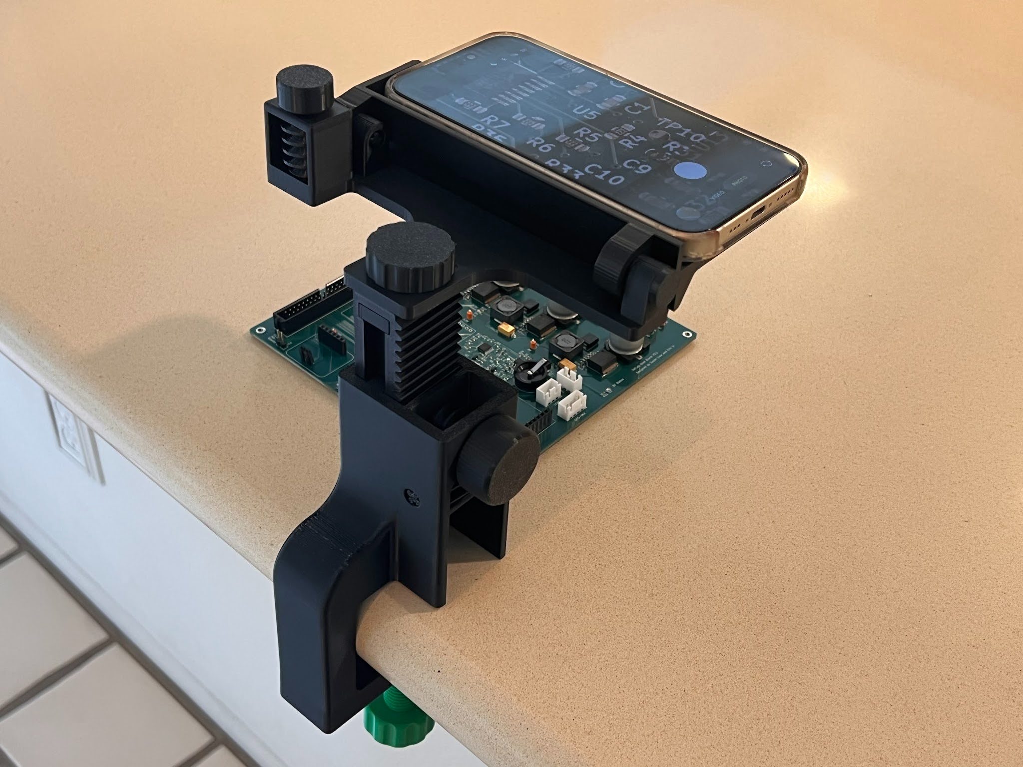
Smartphone Microscope Stand
Turn your phone into a simple digital microscope. Great for soldering and macro photography. Easily adjustable.
View on: